Oxide semiconductor film and method for producing same

a technology of oxidized semiconductor and film, which is applied in the direction of coatings, chemistry apparatus and processes, transistors, etc., can solve the problems of affecting film-formation, rh/sub>2/sub>o/sub>3/sub>was difficult to be formed into a single crystal, and no reports of any success in forming a p-type semiconductor, etc., and achieves the effect of sufficient electrical conductivity

Active Publication Date: 2019-05-23
FLOSFIA
View PDF5 Cites 2 Cited by
  • Summary
  • Abstract
  • Description
  • Claims
  • Application Information

AI Technical Summary

Benefits of technology

[0014]The oxide semiconductor film of a present inventive subject matter is sufficient in electrical conductivity and p-type semiconductor property. The method of manufacturing an oxide semiconductor film is capable of producing the above-mentioned oxide semiconductor film industrially advantageously.

Problems solved by technology

In fact, there has been no reports of any success in forming a p-type semiconductor by use of the methods disclosed in PTLs 1 and 2.
Nevertheless, Rh2O3 was difficult to be formed into a single crystal even when an organic solvent is used, because raw material concentration for Rh2O3 tends to be diluted especially during film-formation that may cause a problem affecting film-formation.
Furthermore, electron density of Rh2O3 was too high.
Also, ZnRh2O4 was insufficient for LED devices and power devices due to low mobility and a narrow band gap.
Therefore, they were not necessarily satisfactory.

Method used


Image

  • Oxide semiconductor film and method for producing same
  • Oxide semiconductor film and method for producing same
  • Oxide semiconductor film and method for producing same

Examples


example

1. Film Formation Apparatus

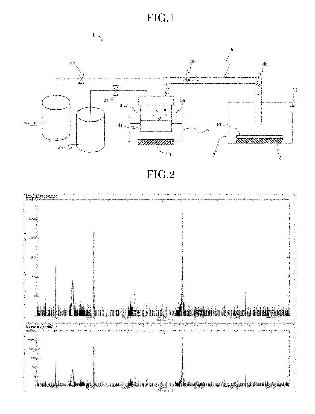
[0053]Regarding a film-formation apparatus, a mist CVD apparatus 1 used in an embodiment of a method according to the present inventive subject matter is described below with FIG. 1. The mist CVD apparatus 1 includes a carrier gas source 2a, a first flow-control valve 3a that is configured to control a flow of carrier gas sent from the carrier gas source 2a, a diluted carrier gas source 2b, a second flow-control valve 3a that is configured to control a flow of diluted carrier gas sent from the diluted carrier gas source 2b, a generator 4 of atomized droplets containing a raw material solution 4a, a vessel 5 containing water 5a, an ultrasonic transducer 6 attached to a bottom of the vessel 5, a film-formation chamber 7, a supply pipe 9 connecting from the generator 4 of atomized droplets to the film-formation chamber 7, a hot plate 8 arranged in the film-formation chamber 7, and an exhaust duct 11 that is configured to exhaust atomized droplets, droplets an...


PUM

PropertyMeasurementUnit
sizeaaaaaaaaaa
sizeaaaaaaaaaa
flow rateaaaaaaaaaa

Abstract

A new and useful oxide semiconductor film with enhanced p-type semiconductor property and the method of manufacturing the oxide semiconductor film are provided. A method of manufacturing an oxide semiconductor film including: generating atomized droplets by atomizing a raw material solution containing a metal of Group 9 of the periodic table and/or a metal of Group 13 of the periodic table and a p-type dopant; carrying the atomized droplets onto a surface of a base by using a carrier gas; causing a thermal reaction of the atomized droplets adjacent to the surface of the base under oxygen atmosphere to form the oxide semiconductor film on the base.

Description

TECHNICAL FIELD[0001]The present invention relates to an oxide semiconductor film that is useful as a p-type semiconductor. Also, the present invention relates to a method for manufacturing an oxide semiconductor film. The present invention also relates to a semiconductor device including an oxide semiconductor film. Furthermore, the present invention relates to a semiconductor system including an oxide semiconductor film.BACKGROUND ART[0002]As a switching device of the next generation achieving high withstand voltage, low losses, and high temperature resistance, semiconductor devices using gallium oxide (Ga2O3) with a large band gap attract attention and are expected to be applied to power semiconductor devices including an inverter. Also, gallium oxide is expected to be applied to a light emitting and receiving element such as a light emitting diode (LED) and a sensor, since gallium oxide has a wide band gap. According to NPL 1, such gallium oxide has a band gap that may be contro...

Claims


Application Information

Patent Timeline
Patent Type & Authority Applications(United States)
IPC IPC(8): H01L29/24C01G55/00H01L35/22H01L21/02H01L33/26
CPCH01L29/24C01G55/002H01L35/22H01L21/02565H01L21/02631H01L33/26C01P2002/54C01P2006/40C01P2006/32C01P2002/70H01L29/872H01L29/778H01L29/7869H01L29/80H01L29/739C01G55/00H01L29/786H01L29/808H01L29/812H01L29/06H01L33/02H01L29/12H01L21/02628H01L21/02579H01L21/0242C23C16/40C23C16/4481H01L29/7813H10N10/855H01L29/78
Inventor TANIKAWA, TOMOCHIKAHITORA, TOSHIMI
Owner FLOSFIA
Why Eureka
Try Eureka