Driving circuit of display panel and driving module thereof, and display device and method for manufacturing the same

a technology of driving circuit and display panel, which is applied in the manufacture of printed circuits, static indicating devices, instruments, etc., can solve the problems of increasing manufacturing costs, and achieve the effect of saving circuit area and cos

Active Publication Date: 2014-07-10
SITRONIX TECH CORP
View PDF7 Cites 6 Cited by
  • Summary
  • Abstract
  • Description
  • Claims
  • Application Information

AI Technical Summary

Benefits of technology

[0007]An objective of the present invention is to provide a driving circuit of a display panel and the driving module thereof, and a display device and the method for manufacturing the same. According to the present invention, a plurality of digital-to-analog converting circuits and a plurality of driving units use different supply voltages provided by the voltage boost circuit and the voltage boost unit, respectively, to shrink the area occupied by the storage capacitor connected externally to the driving circuit or even eliminate the external storage capacitor. Thereby, the purpose of saving circuit area, and hence the purpose of saving costs, can be achieved.

Problems solved by technology

Owing to their huge size, heavy power consumption, and radiation hazardous to the heath of long-term users, traditional CRTs are gradually replaced by liquid crystal displays (LCDs).
Nonetheless, since the capacitance of the storage capacitor is large, 0.1 uF˜4.7 uF approximately, external capacitor device has to be used, leading to an increase of the manufacturing cost.

Method used


Image

  • Driving circuit of display panel and driving module thereof, and display device and method for manufacturing the same
  • Driving circuit of display panel and driving module thereof, and display device and method for manufacturing the same
  • Driving circuit of display panel and driving module thereof, and display device and method for manufacturing the same

Examples


first embodiment

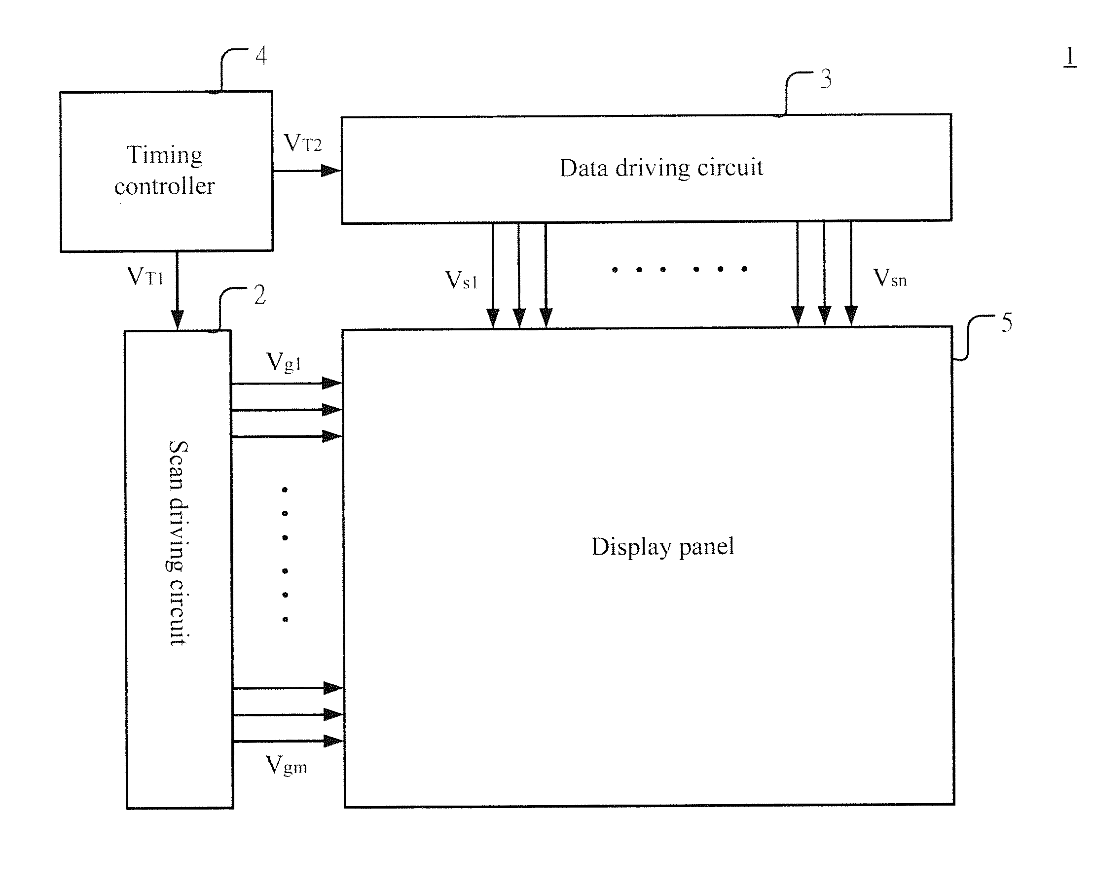
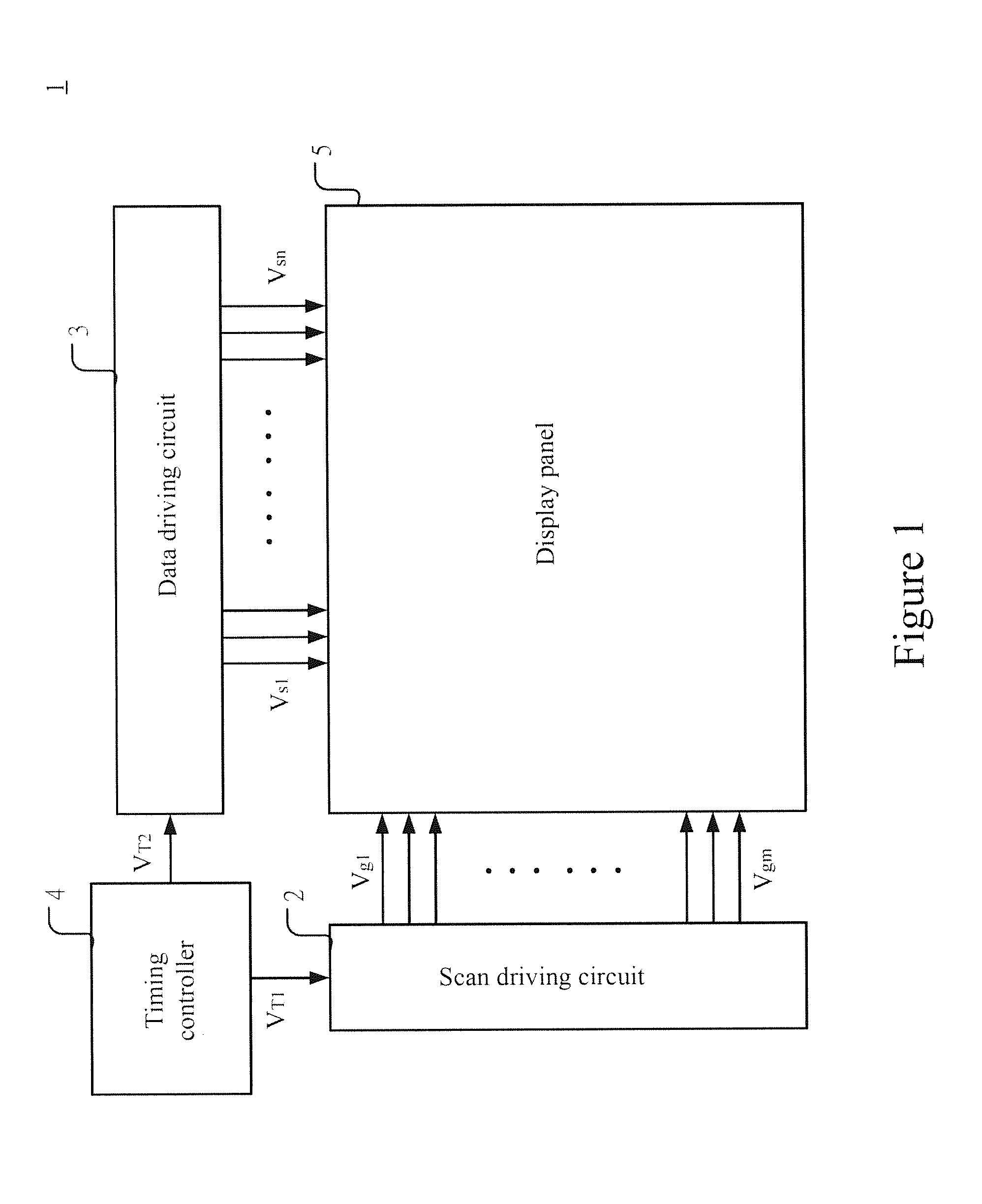
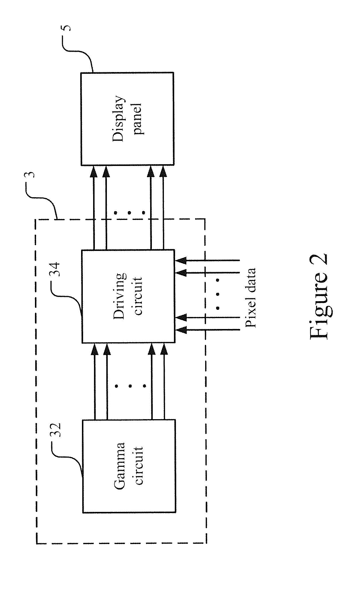
[0036]Please refer to FIG. 4, which shows a block diagram of the driving circuit of the display panel according to the present invention. As shown in the figure, the driving circuit 34 of the display panel 5 according to the present invention comprises a plurality of driving units 340, a plurality of digital-to-analog converting circuits 342, a voltage boost circuit 344, and at least a voltage boost unit 346. The plurality of driving units 340 are coupled to the gamma circuit 32. The plurality of driving units 340 produce a reference driving voltage according to the gamma voltages V1˜Vr of the gamma circuit 32, respectively. Namely, a plurality of output lines of the gamma circuit 32 are coupled to the plurality of driving units 340, respectively. The gamma circuit 32 transmits the plurality of gamma voltages V1˜Vr to the plurality of driving units 340 via the plurality of output lines, drives the plurality of driving units 340 to produce a plurality of reference driving voltages Vr...

second embodiment

[0041]Please refer to FIG. 5, which shows a block diagram of the driving circuit of the display panel according to the present invention. As shown in the figure, the difference between the present embodiment and the one in FIG. 4 is that two voltage boost units 346, 348 are used in the present embodiment. The voltage boost units 346, 348 produce the second supply voltage VP2 and a third supply voltage VP3, respectively. The voltage boost unit 346 transmits the second supply voltage VP2 to first half of the plurality of driving units 340, while the voltage boost unit 348 transmits the third supply voltage VP3 to second half of the plurality of driving units 340. In addition, it is not required that the voltage boost units 346, 348 are responsible for a half of the plurality of driving units 340, respectively. They can be responsible for different proportions of the plurality of driving units 340. For example, the voltage boost unit 346 is responsible for the first one-third of the pl...

fourth embodiment

[0052]Please refer to FIG. 9, which shows a block diagram of the driving circuit of the display panel according to the present invention. As shown in the figure, the difference between the present embodiment and the one in FIG. 6 is that the locations of the plurality of driving units 340 according to the present embodiment and the location of the plurality of digital-to-analog converting circuits 342 are exchanged. In other words, the output of the gamma circuit 32 is coupled to the plurality of digital-to-analog converting circuits 342; the outputs of the plurality of digital-to-analog converting circuits are coupled to the plurality of driving units 340, respectively. Namely, the plurality of digital-to-analog converting circuit 342 receive the plurality of gamma voltages V1˜Vr of the gamma circuit 32 and select one of the plurality of gamma voltages V1˜Vr as a reference driving voltage Vref according to the pixel data, respectively. The plurality of driving units 340 receive the...


PUM

PropertyMeasurementUnit
voltagesaaaaaaaaaa
capacitanceaaaaaaaaaa
gamma voltageaaaaaaaaaa

Abstract

The present invention relates to a driving circuit of a display panel. A plurality of driving units produce a reference driving voltage according to a gamma voltage of a gamma circuit, respectively. A plurality of digital-to-analog converting circuits receive the reference driving voltages output by the plurality of driving units, and select one of the plurality of reference driving voltage as a data driving voltage according to pixel data, respectively. The plurality of digital-to-analog converting circuits transmit the plurality of data driving voltages to the display panel for displaying images. A voltage boost circuit is used for producing a first supply voltage and providing the first supply voltage to the plurality of digital-to-analog converting circuits. At least a voltage boost unit is used for producing a second supply voltage and providing the second supply voltage to the plurality of driving units.

Description

FIELD OF THE INVENTION[0001]The present invention relates generally to a driving circuit and the driving module thereof and to a display device and the method for manufacturing the same, and particularly to a driving circuit of a display panel and the driving module thereof and to a display device and the method for manufacturing the same.BACKGROUND OF THE INVENTION[0002]Modern technologies are developing prosperously. Novel information products are introduced daily for satisfying people's various needs. Early displays are mainly cathode ray tubes (CRTs). Owing to their huge size, heavy power consumption, and radiation hazardous to the heath of long-term users, traditional CRTs are gradually replaced by liquid crystal displays (LCDs). LCDs have the advantages of small size, low radiation, and low power consumption, and thus becoming the mainstream in the market.[0003]In addition, thanks to the rapid advancement of fabrication technologies for panels in recent years, the manufacturin...

Claims


Application Information

Patent Timeline
Patent Type & Authority Applications(United States)
IPC IPC(8): G09G3/36H05K3/30
CPCH05K3/30G09G3/3696Y10T29/4913G09G2310/027G09G2310/0289
Inventor LIAO, MIN-NANSU, CHIH-PING
Owner SITRONIX TECH CORP
Why Eureka
Try Eureka