ESD protection circuit with a stack-coupling device

a protection circuit and stack-coupling technology, applied in emergency protection circuit arrangements, emergency protection circuit arrangements for limiting excess voltage/current, transistors, etc., can solve problems such as circuit lack flexibility, excessive circuit area, and damage to internal circuitry of integrated circuits, so as to improve the esd-preventing ability of esd protection circuits, optimize esd-preventing ability, and enhance esd-preventing ability

Inactive Publication Date: 2005-04-21
REALTEK SEMICON CORP
View PDF5 Cites 4 Cited by
  • Summary
  • Abstract
  • Description
  • Claims
  • Application Information

AI Technical Summary

Benefits of technology

[0007] It is therefore one of the objects of the claimed invention to provide an ESD protection circuit installed with a stack-coupling device to enhance ESD-preventing ability and to solve the above-mentioned problems.
[0008] According to the claimed invention, a stack-coupling device is installed in the ESD protection circuit to improve the ESD-preventing ability of the ESD protection circuit. An OFF duration of the coupling transistor can be adjusted by the stack-coupling device. Moreover, a composite discharging resistance of the stack-coupling device can also be properly arranged.
[0009] In the ESD protection circuit according to the embodiments of the present invention, we utilize a stack-structure coupling device to control the gate voltage of a clamping device to optimize the ESD-preventing ability. In the stack-coupling device, at least two coupling transistors are installed in order to achieve an appropriate OFF duration of the coupling transistors. In addition, regarding the conducted coupling transistors in series connection, an appropriate composite discharging resistance can be achieved to acquire optimized coupling-voltage variation curve and to increase the flexibility of the ESD protection circuit. Since the stack-coupling device has larger composite discharging resistance, under the same coupling-voltage variation curve, the stack-coupling device of the present invention can save more circuit area that that according to the prior art.

Problems solved by technology

Electrical charges caused by electrostatic discharge (ESD) effects may destroy internal circuitry of an integrated circuit.
However, the snap-back effect in the transistor MC has to be triggered by a p-n junction breakdown, and a corresponding trigger voltage may be high enough to cause damage.
However, when the prior-technique utilizes the structure shown in FIG. 2 to provide delay effect, the resistor R and the capacitor C installed in the circuit lack flexibility and the RC combination brings excessive circuit area to increase the cost.

Method used


Image

  • ESD protection circuit with a stack-coupling device
  • ESD protection circuit with a stack-coupling device
  • ESD protection circuit with a stack-coupling device

Examples


Embodiment Construction

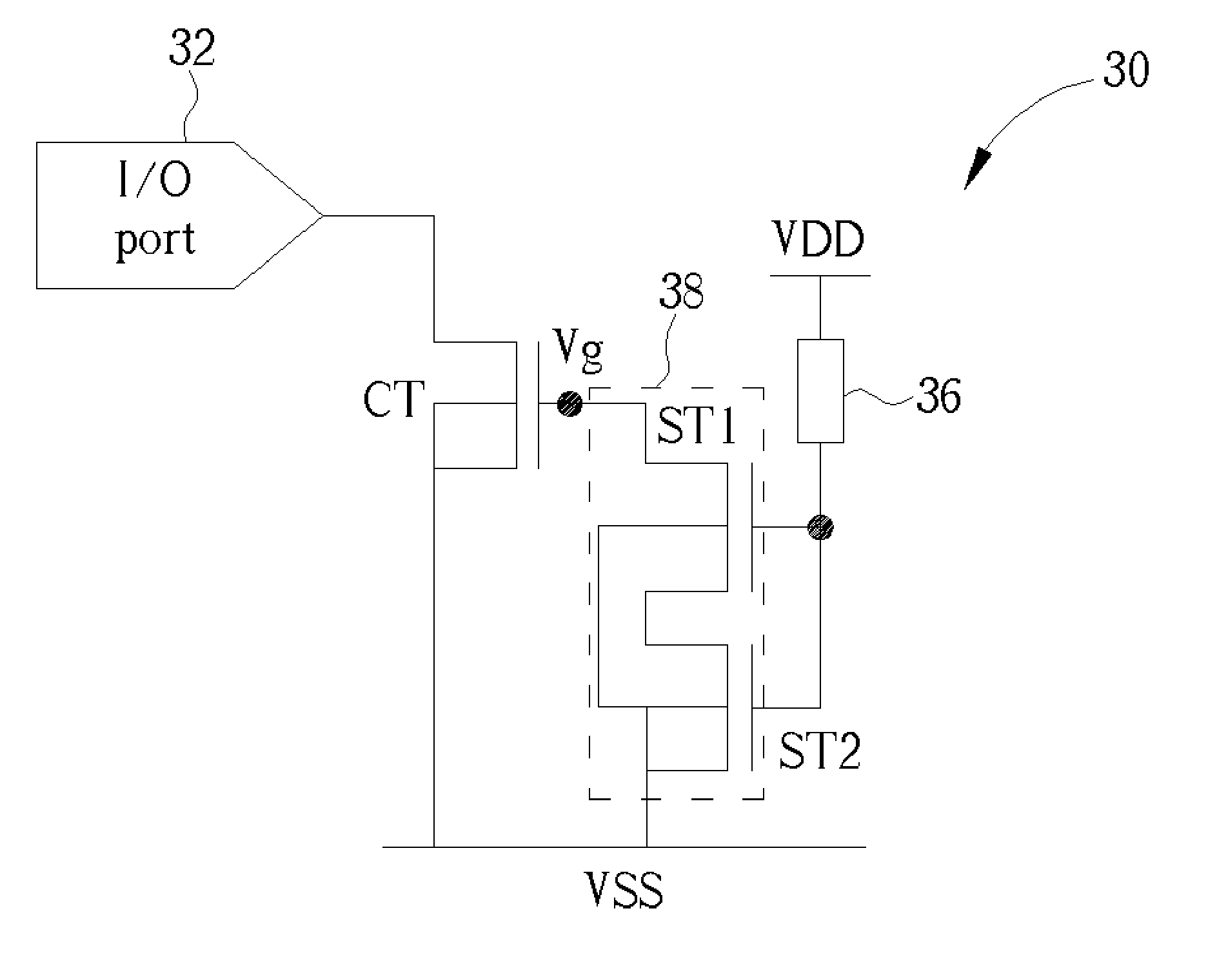
[0018] Embodiments related to the ESD protection circuits according to the present invention include various types. The ESD protection circuits of various types are respectively installed among an I / O port, a high-level voltage source VDD, and a grounding voltage source VSS in a circuit system. Those ESD protection circuits have similar internal structures. Please refer to FIG. 3, which is a schematic diagram of a first embodiment of an ESD protection circuit 30 of the present invention. The ESD protection circuit 30 is installed between an I / O port 32 and a grounding voltage source VSS. The ESD protection circuit 30 includes a clamping transistor CT, a first coupling transistor ST1, a second coupling transistor ST2, and a resistive device 36. In the present embodiment, the clamping transistor CT, the first coupling transistor ST1, and the second coupling transistor ST2 are respectively implemented with a MOS transistor, including a PMOS or an NMOS transistor. The source and the dra...


PUM


Abstract

An ESD protection circuit installed among a plurality of reference nodes includes a clamping device coupled between two reference nodes among the plurality of reference nodes; a stack-coupling device coupled between the clamping device and one of the reference nodes; and at least a resistive device coupled between the stack-coupling device and another one of the reference nodes.

Description

BACKGROUND OF INVENTION [0001] 1. Field of the Invention [0002] The invention relates to an ESD protection circuit, and more particularly, to an ESD protection circuit installed with a stack-coupling device. [0003] 2. Description of the Prior Art [0004] Electrical charges caused by electrostatic discharge (ESD) effects may destroy internal circuitry of an integrated circuit. In order to solve the problem caused by the ESD effect, an ESD protection circuit is set to couple with at least an I / O port and a voltage source (VDD / VSS). When the ESD effect occurs, the ESD protection circuit has to provide a low-resistance discharge path so that the ESD pulses with extremely high peak values can be discharged through the low-resistance discharge path without destroying the internal circuitry. In addition, when the circuit normally operates, the ESD protection circuit should not affect operations of the circuit. [0005] MOS transistors are generally and widely used in ESD protection circuits, ...

Claims


Application Information

Patent Timeline
Patent Type & Authority Applications(United States)
IPC IPC(8): H01L27/04H01L21/822H01L23/60H01L27/02H01L27/06H02H9/00
CPCH01L27/0266
Inventor LIN, YUNG-HAOTSAUR, TAY-HERYEH, TA-HSUNLEE, CHAO-CHENG
Owner REALTEK SEMICON CORP
Why Eureka
Try Eureka