

Sensor and method for manufacturing sensor
a sensor and manufacturing method technology, applied in the direction of paper/cardboard containers, semiconductor/solid-state device details, instruments, etc., can solve the problems of sensor likely to be affected by electromagnetic noise, and reduction of the s/n ratio of electrical signals, so as to prevent a reduction in the s/n ratio and structure , the effect of high quality
- Summary
- Abstract
- Description
- Claims
- Application Information
AI Technical Summary
Benefits of technology
Problems solved by technology
Method used
Image

Examples
first embodiment
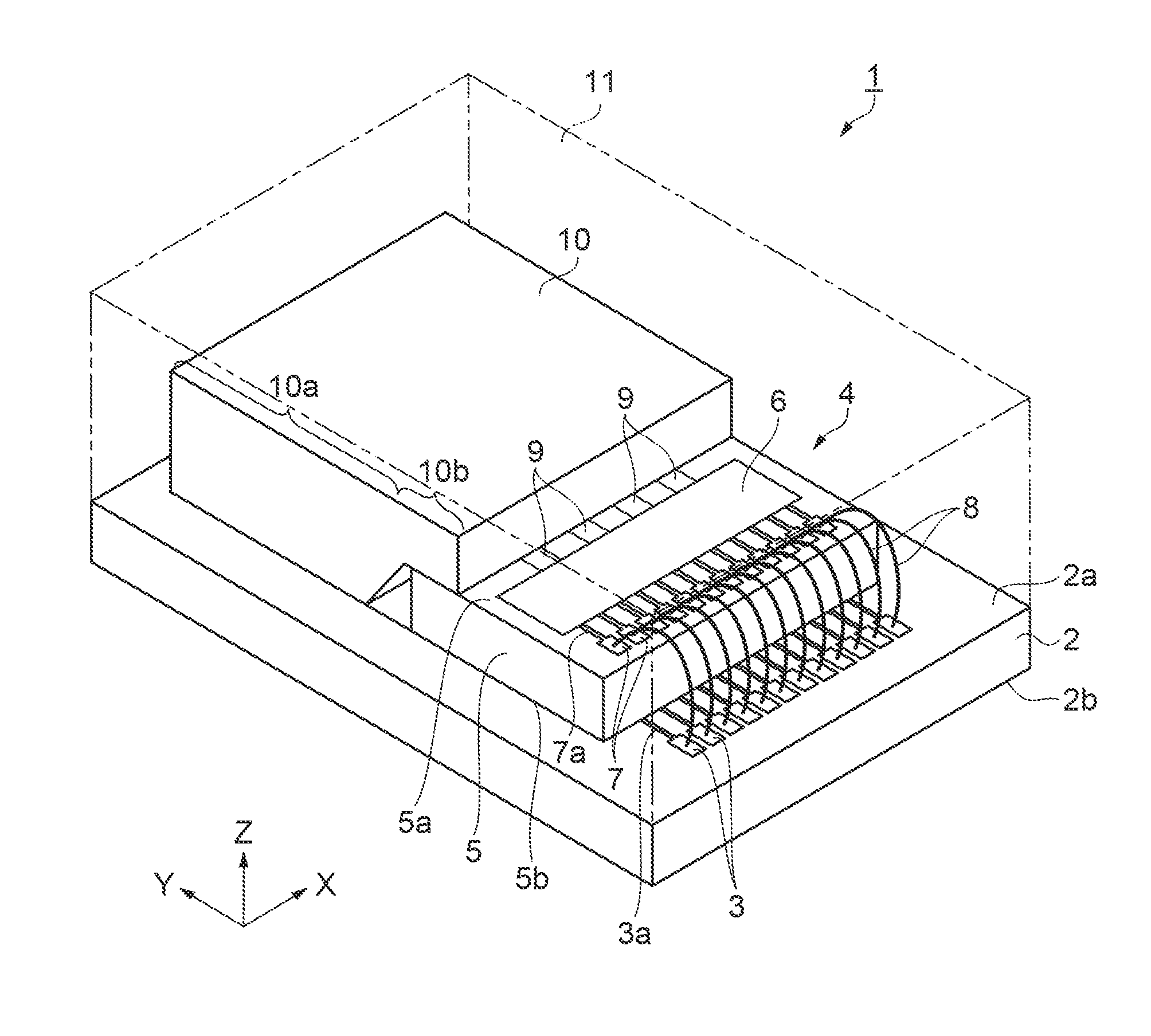
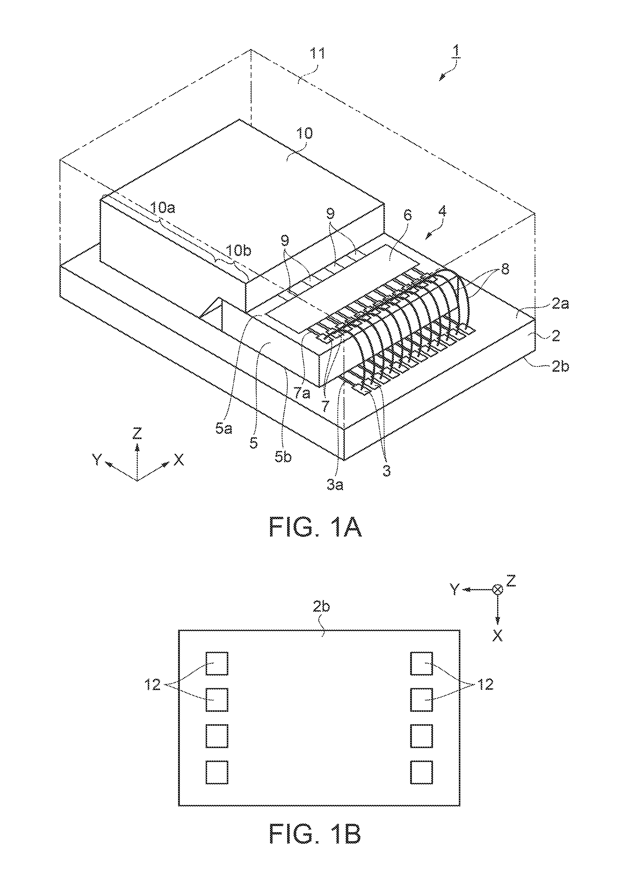
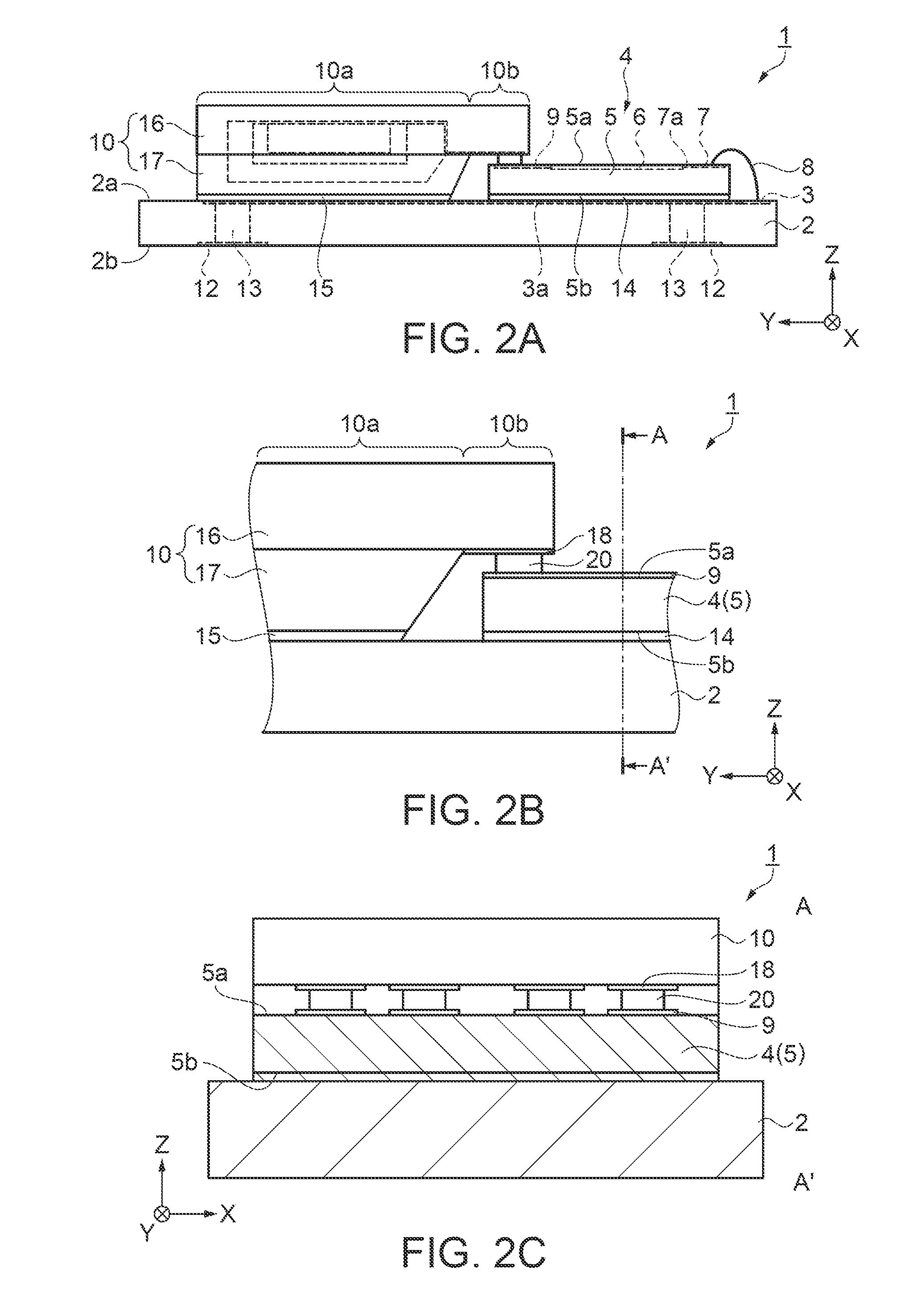
[0034]A sensor and a method for manufacturing the sensor according to a first embodiment will be described according to FIGS. 1A to 6D. FIG. 1A is a schematic perspective view showing the structure of the sensor. FIG. 1B is a schematic bottom plan view showing the structure of the sensor. As shown in FIG. 1A, the sensor 1 includes a rectangular substrate 2. A longitudinal direction of the substrate 2 is defined as a Y-direction. A direction orthogonal to the Y-direction in a planar direction of the substrate 2 is defined as an X-direction. A thickness direction of the substrate 2 is defined as a Z-direction.
[0035]A surface of the substrate 2 on a positive Z-direction side is a top surface 2a, and a surface of the substrate 2 on a negative Z-direction side is a back surface 2b. Twelve input terminals 3 are arranged in parallel in the X-direction on a negative Y-direction side of the top surface 2a. A wiring 3a is connected to each of the input terminals 3.
[0036]The material of the su...
second embodiment
[0082]Next, another embodiment of a sensor will be described with reference to FIG. 7, which is a main part schematic side view of the sensor. A second embodiment differs from the first embodiment in that a through-electrode is disposed in an active chip substrate of an active chip. The description of the same points as those of the first embodiment is omitted.
[0083]In the embodiment, as shown in FIG. 7, a sensor 30 includes the substrate 2. An active chip 31 is disposed on the top surface 2a of the substrate 2 via the thermosetting adhesive 14. The active chip 31 includes an active chip substrate 32. A surface of the active chip substrate 32 facing the positive Z-direction side is a top surface 32a, and a surface of the active chip substrate 32 facing the negative Z-direction side is a back surface 32b. The active chip substrate 32 is a silicon substrate. The semiconductor circuit 6 and intermediate terminals 33 through which input / output signals of the semiconductor circuit 6 are ...
modified example 1
[0089]In the first embodiment, the substrate 2 and the passive chip 10 are bonded together using the thermosetting adhesive 15. Further, the substrate 2 and the active chip 4 are bonded together using the thermosetting adhesive 14. Instead of a thermosetting adhesive, a die attach sheet may be used. The die attach sheet is one of thermosetting adhesives. With the use of the die attach sheet, the active chip 4 or the passive chip 10 can be fixed on the substrate 2 with good workability.
PUM
| Property | Measurement | Unit |
|---|---|---|
| current | aaaaa | aaaaa |
| voltage | aaaaa | aaaaa |
| current | aaaaa | aaaaa |
Abstract
Description
Claims
Application Information