
Electro luminescence panel and method for manufacturing electro luminescence panel

a technology of electroluminescence and electroluminescence, which is applied in the direction of organic semiconductor devices, solid-state devices, thermoelectric devices, etc., can solve the problems of organic el layer degradation, dead spots or dark spots, and pixel degradation, so as to slow down the reduction of the light emission lifetime of the organic el layer

Active Publication Date: 2014-07-31
JOLED INC
View PDF7 Cites 2 Cited by
  • Summary
  • Abstract
  • Description
  • Claims
  • Application Information

AI Technical Summary

Benefits of technology

The present invention relates to an organic EL panel and its manufacturing method. The invention aims to slow down the reduction of the organic EL layer's light emission lifetime, and to allow for the repair of short-circuit defects.

Problems solved by technology

The organic EL element becomes defective due to a short circuit of the upper electrode and the lower electrode which occurs when, for example, a conductive foreign substance attaches to or enters the element during its manufacturing process.
When the defective and abnormal element is included in a pixel, the pixel becomes defective and appears to be a dead spot or a dark spot.

Method used


Image

  • Electro luminescence panel and method for manufacturing electro luminescence panel
  • Electro luminescence panel and method for manufacturing electro luminescence panel
  • Electro luminescence panel and method for manufacturing electro luminescence panel

Examples


Embodiment Construction

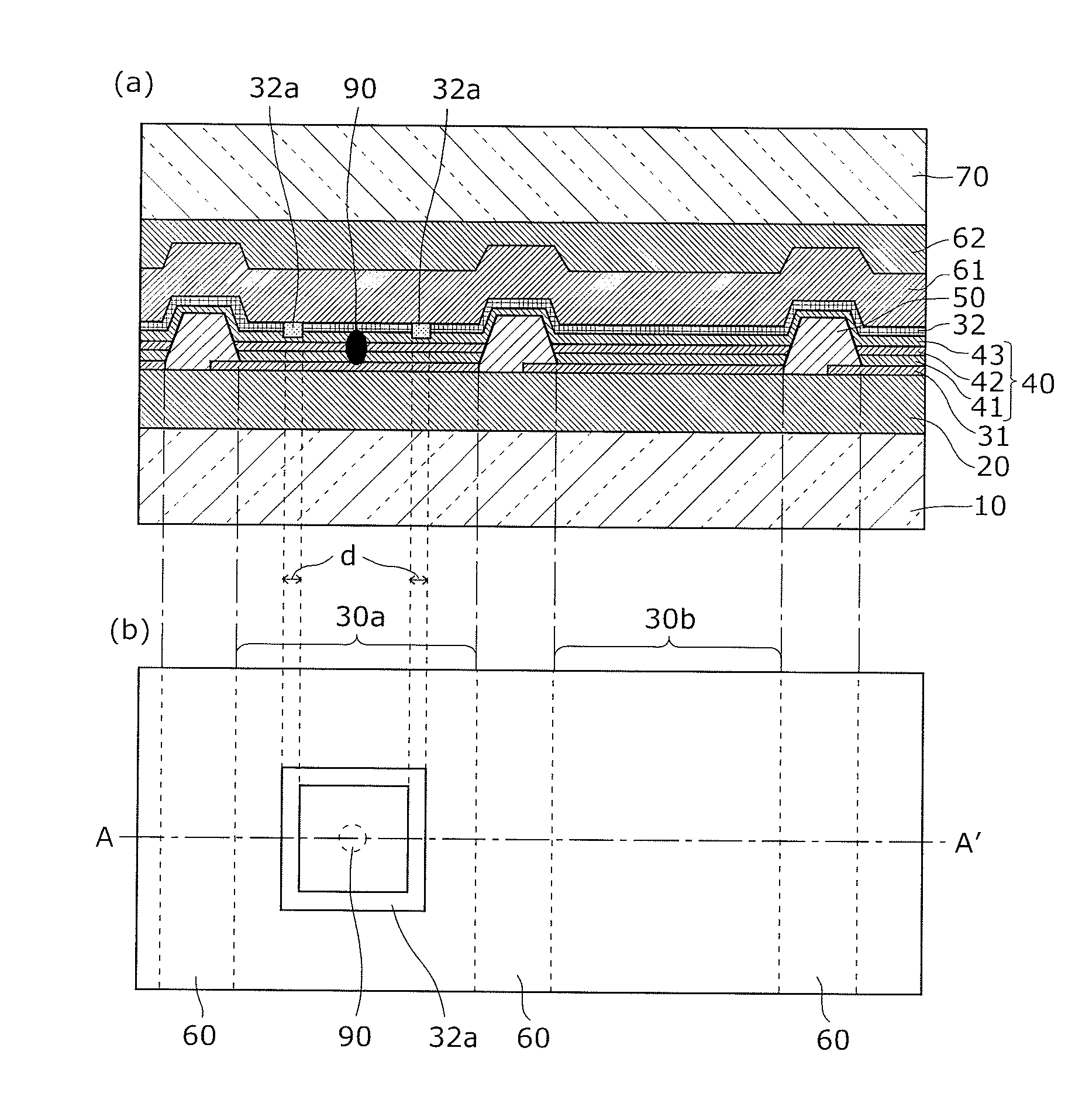
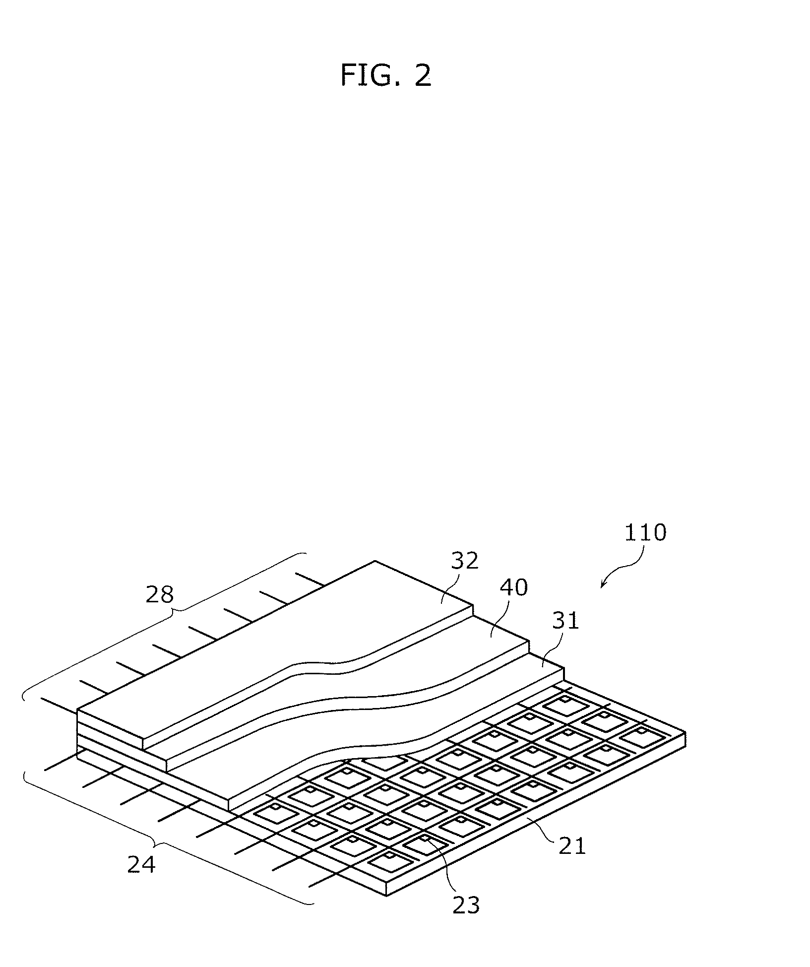
[0026]An organic EL panel according to an implementation of the present invention includes organic EL elements arranged in a matrix and each including an anode, a cathode, and an organic EL layer provided between the anode and the cathode. The organic EL elements include: an abnormal element including: a short-circuit portion at which the anode and the cathode short-circuit; and a resistive portion which is (i) formed to be highly resistive by irradiating at least one of the anode, the organic EL layer, and the cathode with a laser beam, and (ii) positioned on a current pathway between the short-circuit portion and one of the anode and the cathode; and a normal element which does not include the short-circuit portion, in the normal element, the organic EL layer (i) emits light when a voltage higher than or equal to a first voltage is applied between the anode and the cathode, and (ii) does not emit light when a voltage lower than the first voltage is applied between the anode and th...


PUM

PropertyMeasurementUnit
thicknessaaaaaaaaaa
thicknessaaaaaaaaaa
thicknessaaaaaaaaaa

Abstract

The present invention provides an organic EL panel and a manufacturing method of the organic EL layer which can slow the reduction in the light emission lifetime of an organic layer and allow a short-circuit defect to be repaired. Organic EL elements include: an organic EL element including a short-circuit portion, and an altered portion formed to be highly resistive by irradiating a cathode with a laser beam; and an organic EL element which does not include the short-circuit portion. In the organic EL element, an organic EL layer emits light when a voltage higher than or equal to a first voltage is applied. In the organic EL element, the organic EL layer emits light when a voltage higher than equal to a second voltage that is higher than the first voltage is applied.

Description

TECHNICAL FIELD[0001]The present invention relates to an organic electroluminescence (hereinafter referred to as “organic EL”) panel including EL elements, and a method for manufacturing the organic EL panel. In particular, the present invention relates to a technique to repair a short-circuit defect in the organic EL panel.BACKGROUND ART[0002]A conventional organic EL element includes an organic EL layer formed between an upper electrode working as a cathode and a lower electrode working as an anode. The organic EL element becomes defective due to a short circuit of the upper electrode and the lower electrode which occurs when, for example, a conductive foreign substance attaches to or enters the element during its manufacturing process. When the defective and abnormal element is included in a pixel, the pixel becomes defective and appears to be a dead spot or a dark spot.[0003]Here, several known techniques are used to repair such a defective pixel by irradiating an abnormal eleme...

Claims


Application Information

Patent Timeline
Patent Type & Authority Applications(United States)
IPC IPC(8): H01L51/56H01L27/32
CPCH01L27/3241H01L51/56H10K59/12H10K2102/341H10K71/861H10K59/80522H10K71/00H10K50/82H10K50/824H10K59/10
Inventor HIRAOKA, TOMOMISEGAWA, YASUO
Owner JOLED INC
Learn More