Structure and method for reducing source line resistance of light emitting diode

a technology of light-emitting diodes and source lines, which is applied in the field of structure and method can solve the problems of reducing the resistance of source lines, and achieve the effects of reducing the resistance, reducing the resistance, and reducing the voltage drop across the source lin

Active Publication Date: 2007-06-19
AU OPTRONICS CORP
View PDF8 Cites 0 Cited by
  • Summary
  • Abstract
  • Description
  • Claims
  • Application Information

AI Technical Summary

Benefits of technology

[0012]The present invention provides a structure and a method for reducing source line resistance. A conductive layer and the source line are connected in parallel to reduce the resistance, such that the voltage drop across the source line is reduced. Therefore, the voltage distribution of the pixel is more uniform, and the problem of non-uniform brightness is improved.
[0013]The present invention provides a structure and a method for reducing source line resistance, so as to improve uniformity of driving voltage for each pixel of the panel. Therefore, the power consumption is reduced. Further, the corresponding current uniformity and power consumption can also be improved.
[0014]The design of the present invention reduces the source line resistance without changing the material of the source line. The parallel connecting structure can be disposed at the source sensitive area to reduce the voltage drop of the power source.
[0015]The present invention provides a structure for reducing source line of a light emitting display that comprises at least a light emitting diode, a power source and a source line which supplies required power source for driving the light emitting diode. An insulation layer is formed on at least a part of the source line. The insulation layer includes at least two openings exposing the source line structure. A conductive layer is formed to cover the insulation layer and electrically connected to the source line through the openings. The conductive layer and the source line thus are partly connected in parallel. The parallel connection between the conductive layer and the source line thus reduces the resistance of the source line.
[0016]The present invention provides a method for reducing source line resistance of a light emitting display in which a plurality of pixels is formed. Each of the pixels comprises a light emitting diode and a source line to lead a power source for supplying the required power for driving the light emitting diode. The method for reducing the source line resistance includes the following steps. An insulation layer is formed on the source line. A plurality of openings is formed in the insulation layer to expose the underlying source line. A conductive layer is formed to cover the insulation layer and fill the openings. Therefore, the conductive layer is in electrical contact with the source line through the openings.

Problems solved by technology

The parallel connection between the conductive layer and the source line thus reduces the resistance of the source line.

Method used


Image

  • Structure and method for reducing source line resistance of light emitting diode
  • Structure and method for reducing source line resistance of light emitting diode
  • Structure and method for reducing source line resistance of light emitting diode

Examples


Embodiment Construction

[0024]The present invention is characterized in connecting a conductive layer and at least a part of a source line in parallel to reduce the source line resistance, so as to reduce the voltage drop of the driving voltage supplied from the source line to the pixel.

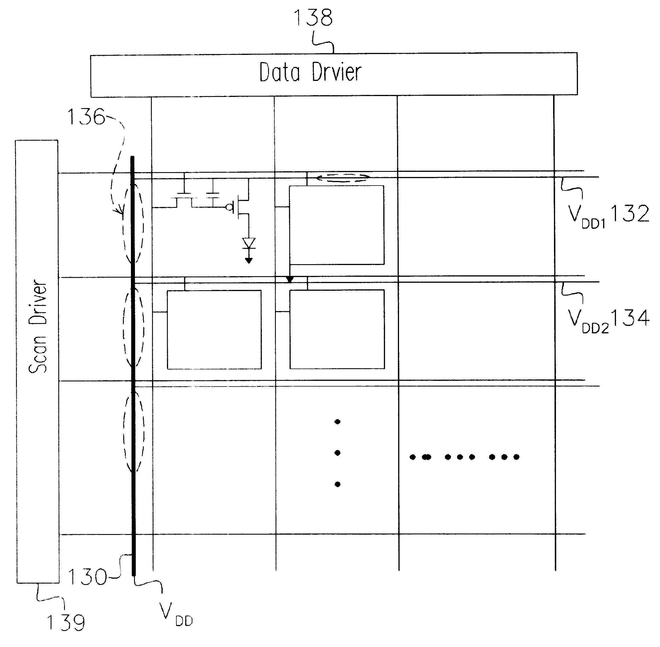
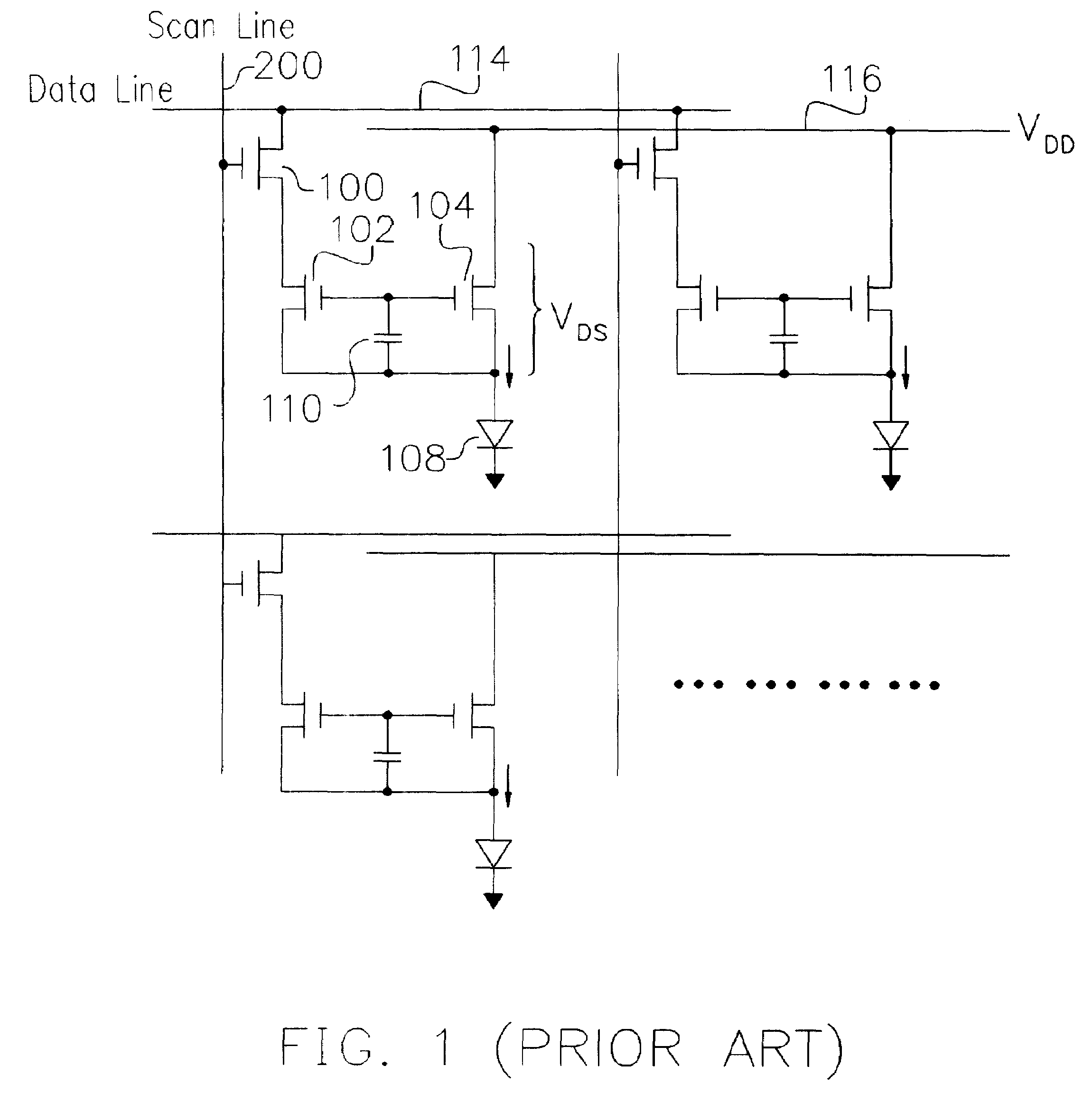
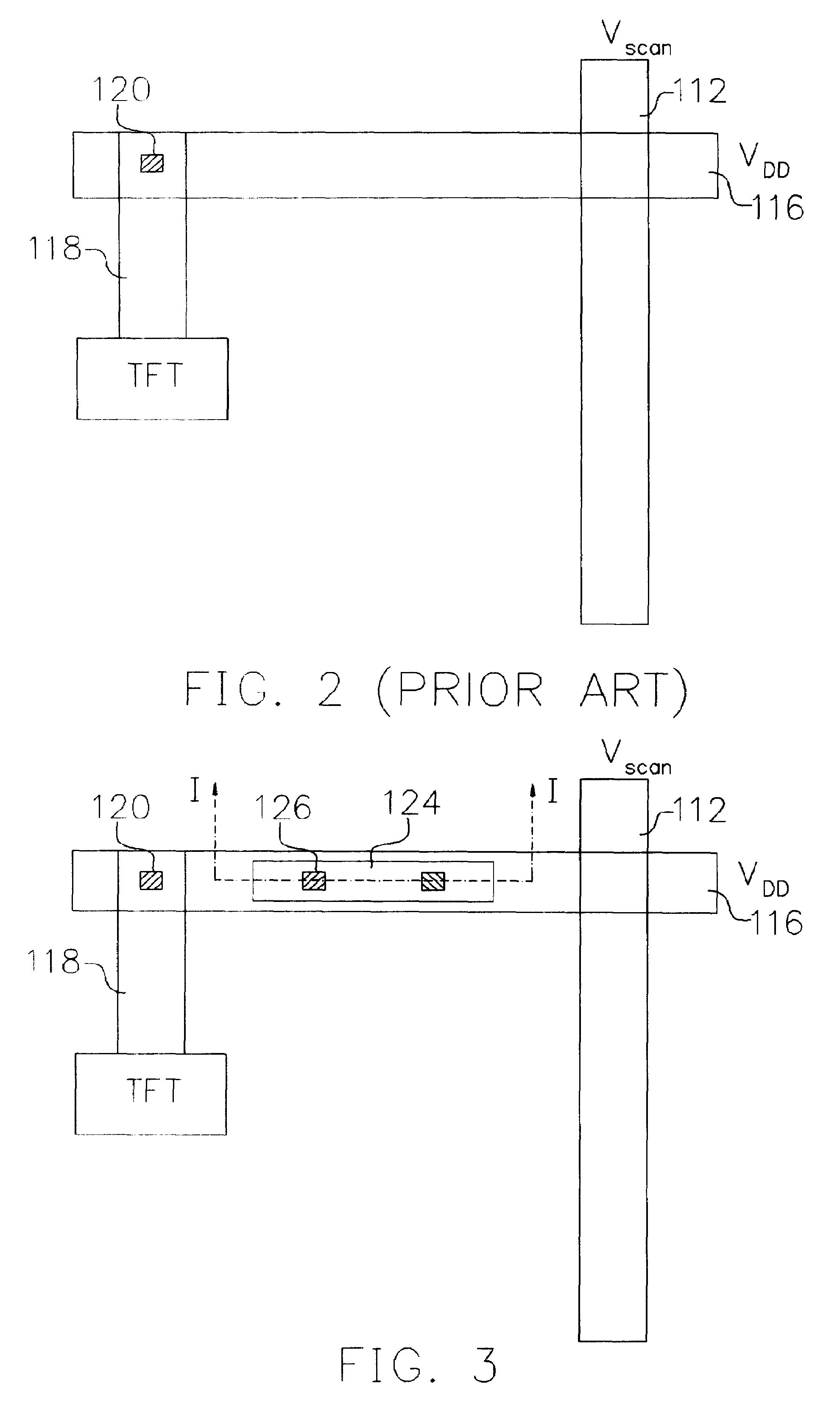
[0025]The driving circuit of a display panel typically comprises scan lines and data lines. To enhance driving speed, the scan lines and the data lines are normally made of materials with lower resistivity such as metal conductors. Meanwhile, the source line is normally made of material with relatively larger resisitivity such as polysilicon. FIG. 3 shows a top view of a source line according to the present invention. To reduce the source line resistance, an additional conductive layer is formed without introducing additional photolithography masking process. As shown in FIG. 3, a conductive layer 124 is electrically connected with a source line 116 in parallel via a plug 126. FIG. 4 shows a cross-sectional view along line ...


PUM


Abstract

A structure and a method for reducing source line resistance of a light emitting diode. A light emitting diode display has at least a light emitting diode, a power source and a power source line structure for guiding the power source to provide the required power for driving the light emitting diode. The structure for reducing the source line resistance has an insulation layer formed on at least a part of the source line structure. The insulation layer has at least two openings exposing the source line structure. A conductive layer is formed to cover the insulation layer and is in electrical contact with the source line structure through the openings. Thereby, the conductive layer and the source line are connected in parallel, and the resistance of the source line is thus reduced.

Description

CROSS REFERENCE TO RELATED APPLICATIONS[0001]This application claims the priority benefit of Taiwan application serial no. 91135004, filed Dec. 03, 2002.BACKGROUND OF INVENTION[0002]1. Field of the Invention[0003]The invention relates in general to a light emitting device display technique, and more particularly, to an organic light emitting diode (OLED) for reducing power source resistance. Thereby, a stable and uniform driving voltage is supplied to each pixel of the organic light emitting diode.[0004]2. Related Art of the Invention[0005]Following with the advancement in high-tech, video products, particularly digital video products or image apparatus have become one of the most common products in our daily lives. Among various video products or image apparatus, the display is an important device for information display. The user can read information from a display, or even control the operation of an apparatus.[0006]To compliment the modern life style, the video products or image...

Claims


Application Information

Patent Timeline
Patent Type & Authority Patents(United States)
IPC IPC(8): G09G3/30G09G3/10H01L27/32
CPCH01L27/3276H10K59/131
Inventor HU, JEN-YISUN, WEIN-TOWN
Owner AU OPTRONICS CORP
Why Eureka
Try Eureka