Semiconductor device and method for producing semiconductor device

a semiconductor and semiconductor technology, applied in the direction of semiconductor devices, bulk negative resistance effect devices, electrical appliances, etc., can solve the problems of difficult connection of many transistors to word lines, difficult to make an impurity present in silicon pillars, etc., to reduce the resistance of a source line, reduce the number of steps, and suppress the effect of an increase in source voltag

Active Publication Date: 2015-05-28
UNISANTIS ELECTRONICS SINGAPORE PTE LTD
View PDF4 Cites 10 Cited by
  • Summary
  • Abstract
  • Description
  • Claims
  • Application Information

AI Technical Summary

Benefits of technology

[0053]The semiconductor device includes a fin-shaped semiconductor layer formed on a semiconductor substrate, a first insulating film formed around the fin-shaped semiconductor layer, the first pillar-shaped semiconductor layer formed on the fin-shaped semiconductor layer, and the gate insulating film formed around the gate electrode and the gate line and on bottom portions of the gate electrode and the gate line. The gate electrode is made of a metal and the gate line is made of a metal, the gate line extending in a direction perpendicular to a direction in which the fin-shaped semiconductor layer extends. The second diffusion layer is further formed in the fin-shaped semiconductor layer. The outer width of the gate electrode is equal to the width of the gate line. The width of the first pillar-shaped semiconductor layer is equal to the width of the fin-shaped semiconductor layer. Thus, the fin-shaped semiconductor layer, the pillar-shaped semiconductor layer, the gate electrode, and the gate line of this semiconductor device are formed through a self-aligned process with two masks. This can reduce the number of steps.
[0054]The presence of the contact line which is parallel to the gate line and is connected to the second diffusion layer can reduce the resistance of a source line and can suppress an increase in the source voltage caused by electric current at the time of the set operation. Regarding the contact line which is parallel to the gate line, one contact line is preferably disposed for every 2 memory cells, 4 memory cells, 8 memory cells, 16 memory cells, 32 memory cells, or 64 memory cells arranged in a row in a direction in which the bit line extends.
[0055]A structure constituted by the second pillar-shaped semiconductor layer, the contact electrode formed around the second pillar-shaped semiconductor layer, and the contact line is the same as a transistor structure, except that the contact electrode is connected to the second diffusion layer. All source lines which extend in a direction parallel to a direction in which the gate line extends are connected to the contact line. This can reduce the number of steps.

Problems solved by technology

In bipolar transistors, an electric current flows through a gate and thus it is difficult to connect many transistors to word lines.
As the width of a silicon pillar decreases, it becomes more difficult to make an impurity be present in the silicon pillar because the density of silicon is 5×10²² / cm3.

Method used


Image

  • Semiconductor device and method for producing semiconductor device
  • Semiconductor device and method for producing semiconductor device
  • Semiconductor device and method for producing semiconductor device

Examples


Embodiment Construction

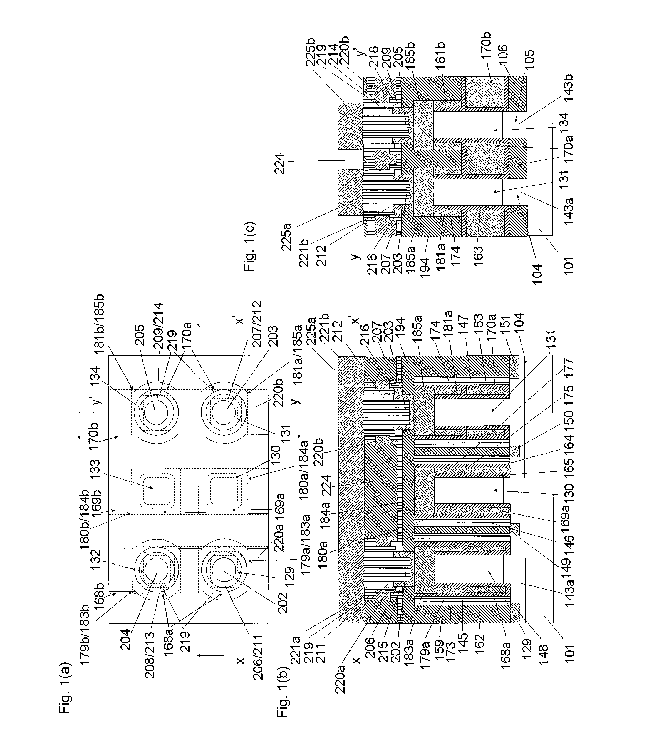
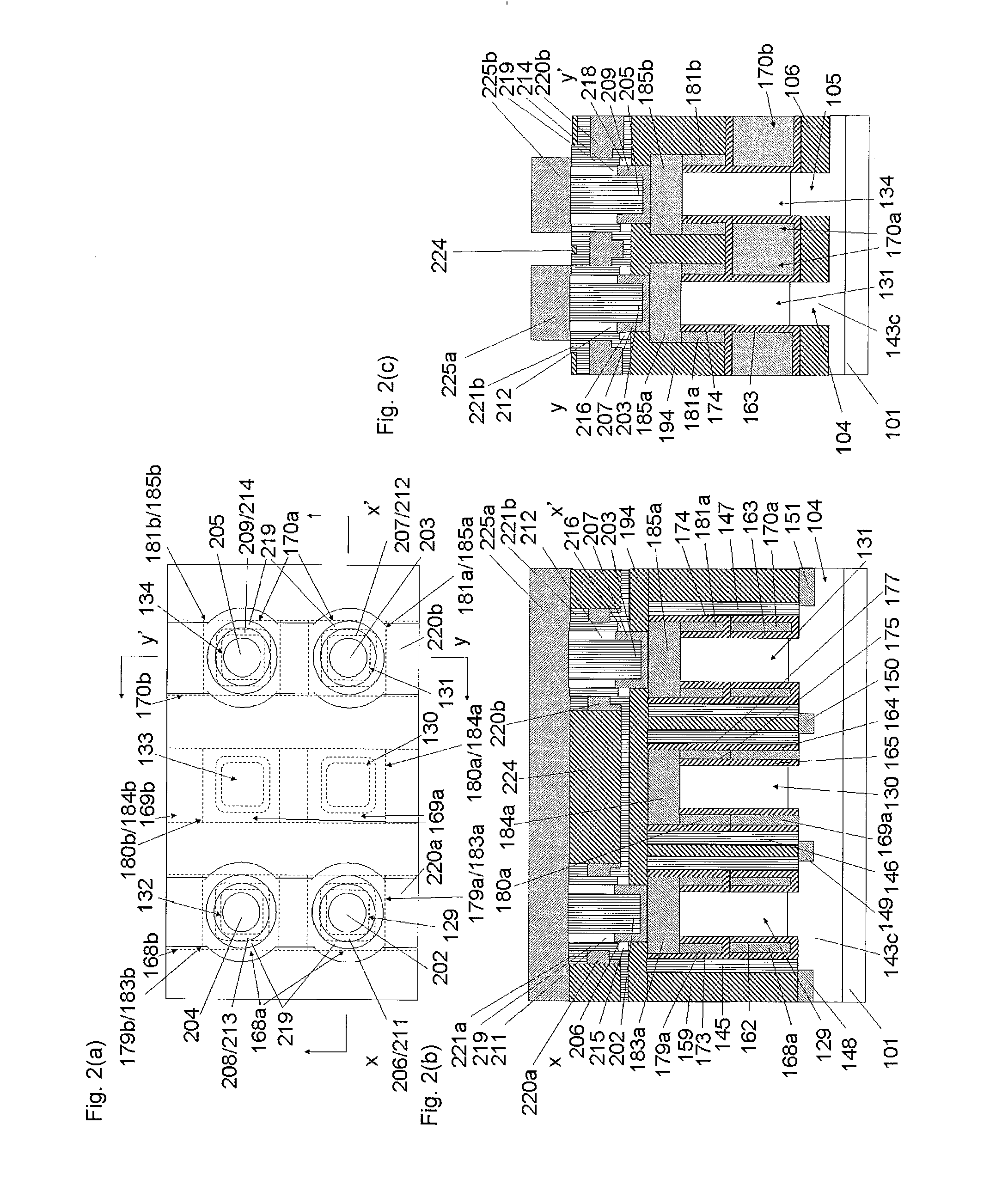
[0125]FIGS. 1(a), 1(b) and 1(c) show a structure of a semiconductor device.

[0126]As shown in FIGS. 1(a), 1(b) and 1(c), memory cells serving as semiconductor devices of the present invention are arranged in a first row and a first column, in a first row and a third column, in a second row and a first column, and in a second row and a third column, and contact devices including a contact electrode and a contact line are arranged in a first row and a second column and in a second row and a second column in order to connect source lines to each other.

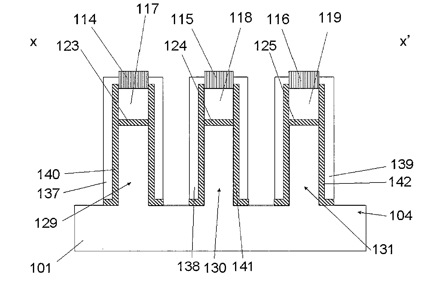
[0127]The memory cell in the second row and the first column includes a fin-shaped semiconductor layer 104 formed on a semiconductor substrate 101; a first insulating film 106 formed around the fin-shaped semiconductor layer 104; a first pillar-shaped semiconductor layer 129 formed on the fin-shaped semiconductor layer 104; a gate insulating film 162 formed around the first pillar-shaped semiconductor layer 129; a gate electrode 168a made ...


PUM

PropertyMeasurementUnit
work functionaaaaaaaaaa
insulatingaaaaaaaaaa

Abstract

The present invention provides a memory structure including a resistance-changing storage element, which enables a reset operation with a reset gate and in which cross-sectional areas of a resistance-changing film and a lower electrode in a current-flowing direction can be decreased. The semiconductor device of the present invention comprises a first pillar-shaped semiconductor layer, a gate insulating film formed around the first pillar-shaped semiconductor layer, a gate electrode made of a metal and formed around the gate insulating film, a gate line made of a metal and connected to the gate electrode, a second gate insulating film formed around an upper portion of the first pillar-shaped semiconductor layer, a first contact made of a second metal and formed around the second gate insulating film, a second contact which is made of a third metal and which connects an upper portion of the first contact to an upper portion of the first pillar-shaped semiconductor layer, a second diffusion layer formed in a lower portion of the first pillar-shaped semiconductor layer, a pillar-shaped insulating layer formed on the second contact, a resistance-changing film formed around an upper portion of the pillar-shaped insulating layer, a lower electrode formed around a lower portion of the pillar-shaped insulating layer and connected to the resistance-changing film, a reset gate insulating film that surrounds the resistance-changing film, and a reset gate that surrounds the reset gate insulating film.

Description

RELATED APPLICATIONS[0001]This application is a continuation application of International Application No. PCT / JP2013 / 081543 filed on Nov. 22, 2013, the entire content of which is incorporated herein by reference.TECHNICAL FIELD[0002]The present invention relates to a semiconductor device and a method for producing a semiconductor device.BACKGROUND ART[0003]In recent years, a phase-change memory has been developed (e.g., refer to PTL 1). A phase-change memory stores information by changing and recording the resistance of an information memory element of a memory cell.[0004]This is caused by a mechanism in which, when an electric current is caused to flow between a bit line and a source line by turning ON a cell transistor, heat is generated by a high-resistance element serving as a heater, chalcogenide glass (GST: Ge2Sb2Te5) that is in contact with the heater is melted, and a state transition occurs. When chalcogenide glass is melted at high temperature (high current) and cooled rapi...

Claims


Application Information

Patent Timeline
Patent Type & Authority Applications(United States)
IPC IPC(8): H01L45/00H01L27/24
CPCH01L45/06H01L27/2454H01L45/1206H01L45/16H10B63/34H10N70/8265H10N70/231H10N70/8413H10N70/068H10B63/30H10N70/021H10N70/011H10N70/063H10N70/253H10N70/823H10N70/841
Inventor MASUOKA, FUJIONAKAMURA, HIROKI
Owner UNISANTIS ELECTRONICS SINGAPORE PTE LTD
Why Eureka
Try Eureka