MAGNETIC RANDOM ACCESS MEMORY (MRAM) BIT CELLS EMPLOYING SOURCE LINES (SLs) AND/OR BIT LINES (BLs) DISPOSED IN MULTIPLE, STACKED METAL LAYERS TO REDUCE MRAM BIT CELL RESISTANCE

a random access memory and bit cell technology, applied in the field of magnetic tunnel junctions, can solve the problems of increasing the number of metal wires, increasing increasing the loss of write current margin, etc., and achieving the effect of reducing the resistance of bit lines, reducing the resistance of source lines, and saving power

Inactive Publication Date: 2016-09-01
QUALCOMM INC
View PDF5 Cites 9 Cited by
  • Summary
  • Abstract
  • Description
  • Claims
  • Application Information

AI Technical Summary

Benefits of technology

[0011]In this regard, in aspects disclosed herein, MRAM bit cells are fabricated in an IC to provide a memory array. In certain aspects disclosed herein, the MRAM bit cells are provided with source lines formed by multiple stacked metal layers disposed above a semiconductor layer to reduce the resistance of the source lines. In other aspects disclosed herein, the bit lines of the MRAM bit cells may also be formed in multiple stacked metal layers disposed above the semiconductor layer to reduce the resistance of the bit lines. In this manner, if the node size in the IC is scaled down, the resistance of the source lines and / or the bit lines can be maintained to maintain the total resistance of the MRAM bit cell read / write path to allow a same, sufficient write current to be generated for write operations for a given drive voltage. Furthermore, if a source line and / or bit line is formed within multiple stacked metal layers in an IC to reduce (rather than maintain) the resistance of the source lines and / or the bit lines, a write driver voltage and / or the IC voltage can be reduced to conserve power while generating a sufficient write current in the MRAM bit cell sufficient for write operations. Or, if it is desired to provide a higher write operating yield for the MRAM bit cell, the resistance of the source lines and / or the bit lines can be reduced without reducing the voltage of the voltage supply to generate an increased write current in the MRAM bit cell.
[0012]Further, in other aspects disclosed herein, to compensate or offset an otherwise resistance imbalance between a source line and a bit line in an MRAM bit cell that results from a typical MRAM bit cell layout in an IC providing narrower source lines than bit lines, the source lines and / or bit lines provided in the MRAM bit cells disclosed herein may be provided in additional metal layers. Providing the source lines and / or bit lines in additional metal layers can further reduce the resistance of the source lines and / or bit lines to provide a greater resistance balance between the source lines and the bit lines in the MRAM bit cells, thereby allowing drive voltage in a write driver circuit to be decreased. This is because resistance imbalance between source lines and bit lines in an MRAM array causes additional loss in write current margin, which have to be provided in a writer driver circuit during write operations to compensate for the resulting increase in the overall resistance difference between MRAM bit cells located nearer and farther away from the write driver circuit. Resistance imbalance between source lines and bit lines in an MRAM array can also increase signal degradation during read operations.

Problems solved by technology

However, the number of metal wires typically increases, because lithography limitations reduce or eliminate free-formed wiring in the IC and demand increases to couple larger numbers of logic gates through interconnections.
This is because resistance imbalance between source lines and bit lines in an MRAM array causes additional loss in write current margin, which have to be provided in a writer driver circuit during write operations to compensate for the resulting increase in the overall resistance difference between MRAM bit cells located nearer and farther away from the write driver circuit.
Resistance imbalance between source lines and bit lines in an MRAM array can also increase signal degradation during read operations.

Method used


Image

  • MAGNETIC RANDOM ACCESS MEMORY (MRAM) BIT CELLS EMPLOYING SOURCE LINES (SLs) AND/OR BIT LINES (BLs) DISPOSED IN MULTIPLE, STACKED METAL LAYERS TO REDUCE MRAM BIT CELL RESISTANCE
  • MAGNETIC RANDOM ACCESS MEMORY (MRAM) BIT CELLS EMPLOYING SOURCE LINES (SLs) AND/OR BIT LINES (BLs) DISPOSED IN MULTIPLE, STACKED METAL LAYERS TO REDUCE MRAM BIT CELL RESISTANCE
  • MAGNETIC RANDOM ACCESS MEMORY (MRAM) BIT CELLS EMPLOYING SOURCE LINES (SLs) AND/OR BIT LINES (BLs) DISPOSED IN MULTIPLE, STACKED METAL LAYERS TO REDUCE MRAM BIT CELL RESISTANCE

Examples


Embodiment Construction

[0029]With reference now to the drawing figures, several exemplary aspects of the present disclosure are described. The word “exemplary” is used herein to mean “serving as an example, instance, or illustration.” Any aspect described herein as “exemplary” is not necessarily to be construed as preferred or advantageous over other aspects.

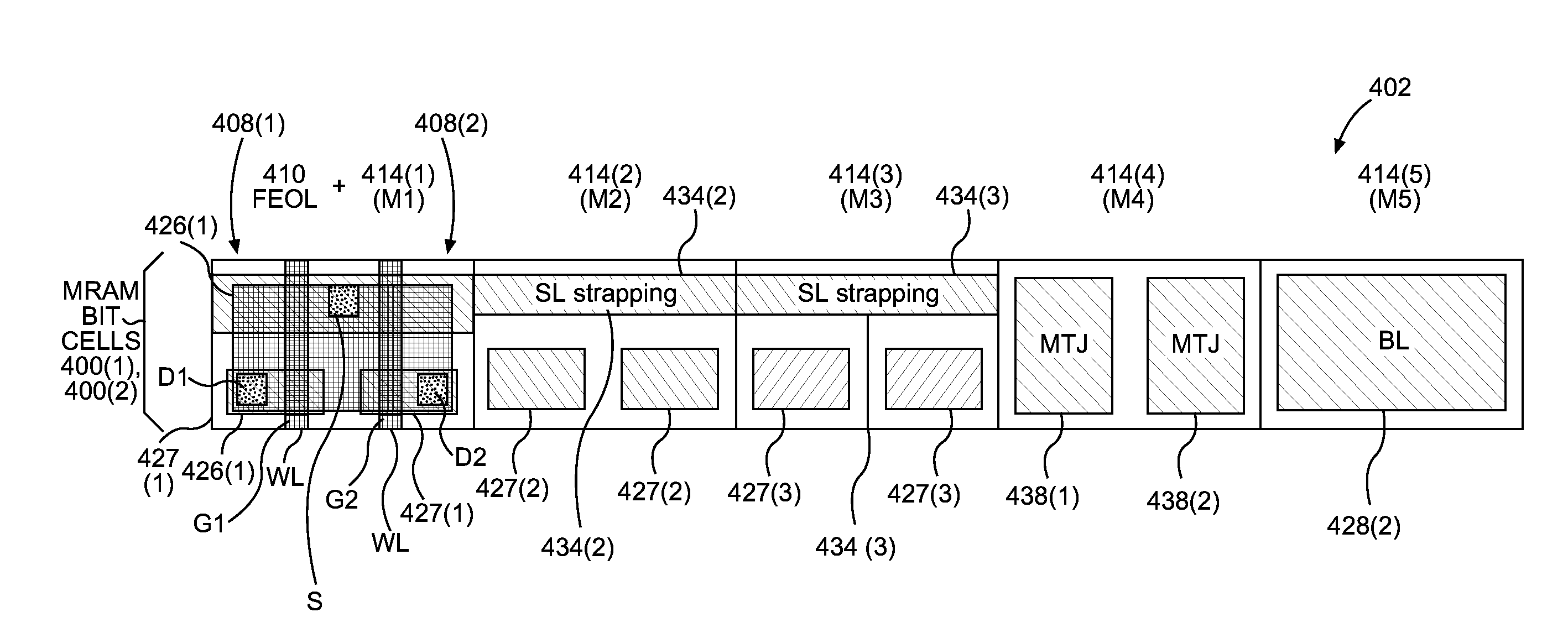
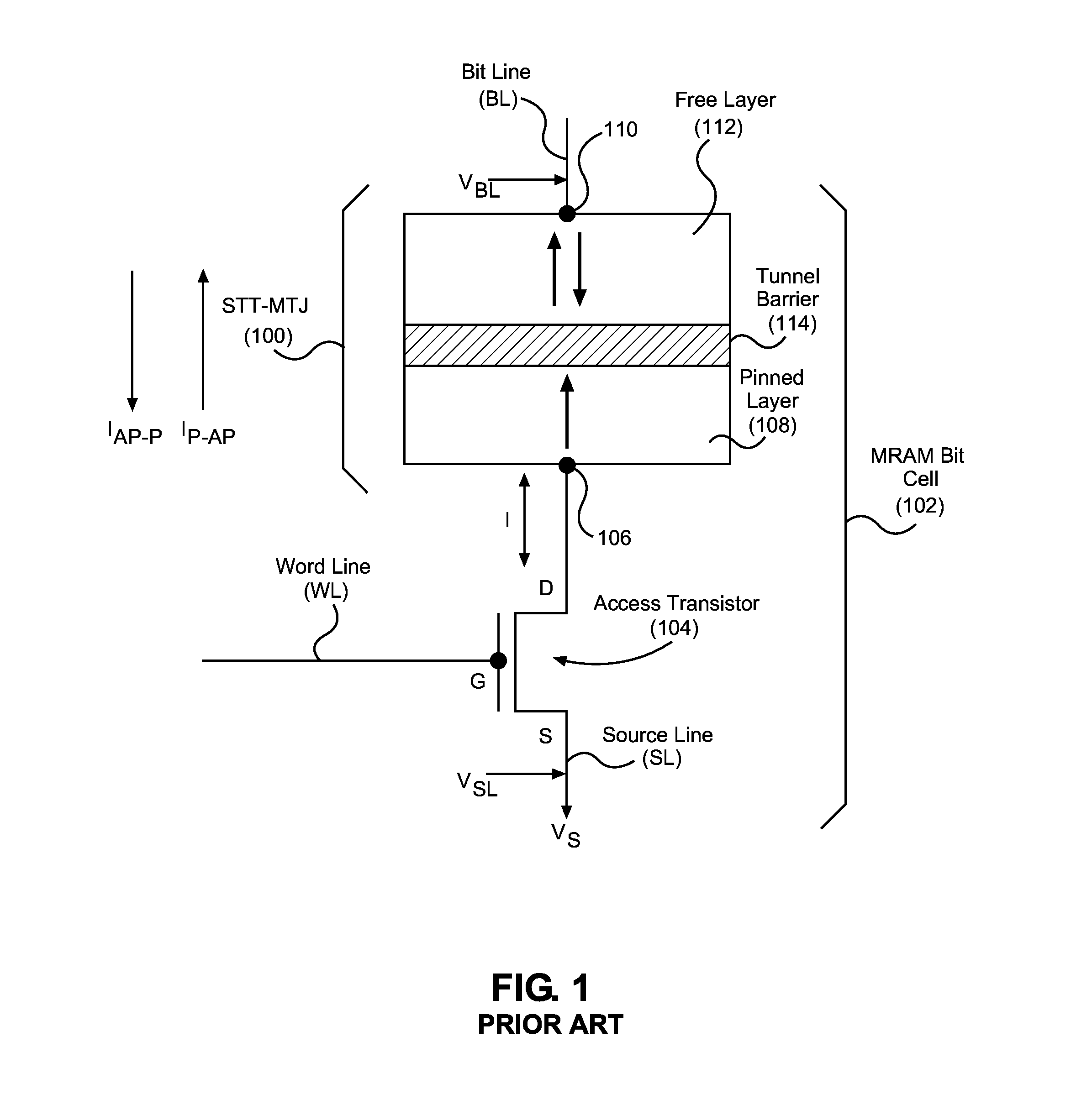
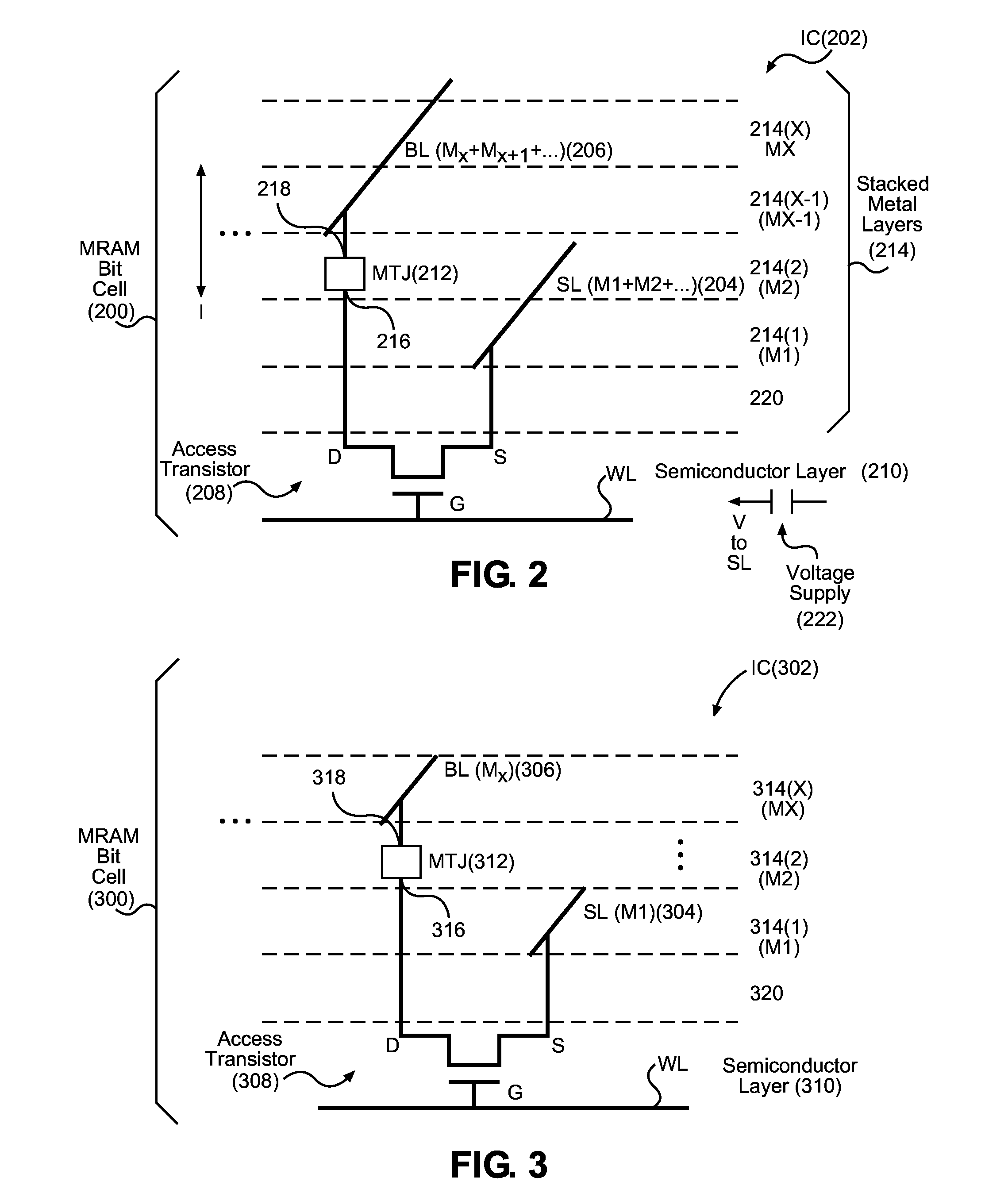
[0030]Aspects of the disclosure involve magnetic random access memory (MRAM) bit cells employing source lines and / or bit lines disposed in multiple, stacked metal layers to reduce MRAM bit cell resistance. Related methods and systems are also disclosed. Metal interconnection resistance of a source line and a bit line in an MRAM bit cell contributes towards the overall resistance of the MRAM bit cell. The resistance of the MRAM bit cell affects the amount of write current generated in the MRAM bit cell for a given voltage applied at an edge of an MRAM array including the MRAM bit cell. As node size is scaled down, metal interconnection resistance incre...


PUM


Abstract

Magnetic random access memory (MRAM) bit cells employing source lines and/or bit lines disposed in multiple, stacked metal layers to reduce MRAM bit cell resistance are disclosed. Related methods and systems are also disclosed. In aspects disclosed herein, MRAM bit cells are provided in a memory array. The MRAM bit cells are fabricated in an integrated circuit (IC) with source lines and/or bit lines formed by multiple, stacked metal layers disposed above a semiconductor layer to reduce the resistance of the source lines. In this manner, if node size in the IC is scaled down, the resistance of the source lines and/or the bit lines can be maintained or reduced to avoid an increase in drive voltage that generates a write current for write operations for the MRAM bit cells.

Description

PRIORITY APPLICATION[0001]The present application claims priority under 35 U.S.C. §119(e) to U.S. Provisional Patent Application Ser. No. 62 / 121,982 filed on Feb. 27, 2015 and entitled “MAGNETIC RANDOM ACCESS MEMORY (MRAM) BIT CELLS EMPLOYING SOURCE LINES (SLs) AND / OR BIT LINES (BLs) DISPOSED IN MULTIPLE, STACKED METAL LAYERS TO REDUCE MRAM BIT CELL RESISTANCE,” which is incorporated herein by reference in its entirety.BACKGROUND[0002]I. Field of the Disclosure[0003]The technology of the disclosure relates generally to magnetic tunnel junctions (MTJs), and more particularly to MTJs employed in magnetic random access memory (MRAM) bit cells to provide MRAM.[0004]II. Background[0005]Semiconductor storage devices are used in integrated circuits (ICs) in electronic devices to provide data storage. One example of a semiconductor storage device is magnetic random access memory (MRAM). MRAM is non-volatile memory in which data is stored by programming a magnetic tunnel junction (MTJ) as pa...

Claims


Application Information

Patent Timeline
Patent Type & Authority Applications(United States)
IPC IPC(8): H01L27/22H01L43/12H01L43/08G11C11/16H01L43/02
CPCH01L27/222G11C11/161H01L43/12H01L43/08H01L43/02H10B61/22H10N50/10H10N50/01G11C11/1659H10B61/00H10N50/80
Inventor LU, YUZHU, XIAOCHUNKANG, SEUNG HYUK
Owner QUALCOMM INC
Why Eureka
Try Eureka