Unlock instant, AI-driven research and patent intelligence for your innovation.

Flash memory and associated programming method

Active Publication Date: 2014-07-31
EMEMORY TECH INC
View PDF1 Cites 1 Cited by
  • Summary
  • Abstract
  • Description
  • Claims
  • Application Information

AI Technical Summary

Benefits of technology

The invention is a flash memory that can program multiple bits of data at once, which reduces the programming time.

Problems solved by technology

Since the conventional flash memory is unable to program multiple bits of data simultaneously, the programming time period of the conventional flash memory is very long.

Method used


Image

  • Flash memory and associated programming method
  • Flash memory and associated programming method
  • Flash memory and associated programming method

Examples


Embodiment Construction

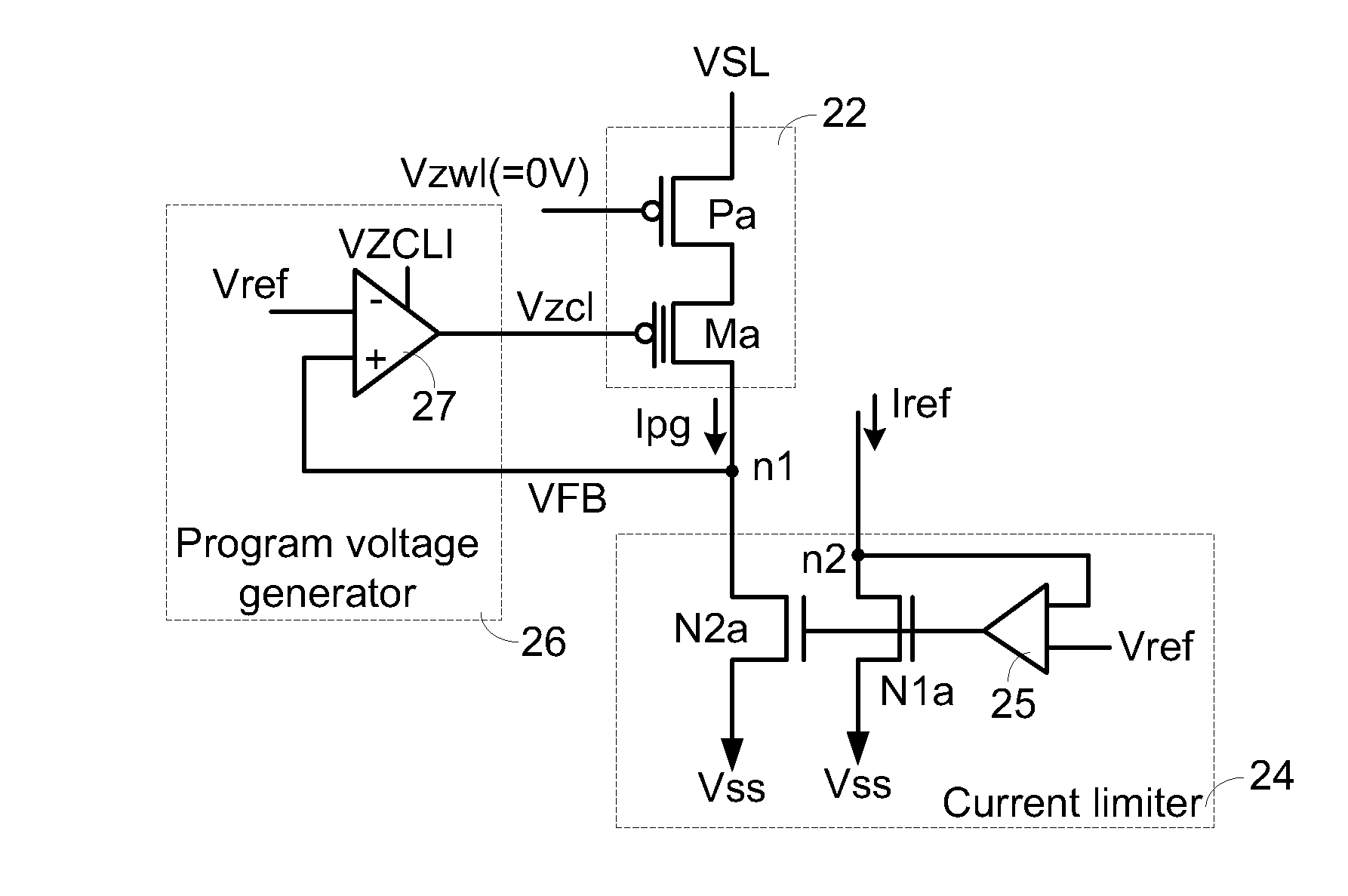
[0020]Hereinafter, a circuit for programming a single memory unit will be illustrated with reference to FIG. 2A. FIG. 2A is a schematic circuit diagram illustrating a programming circuit for programming a single memory unit according to the present invention. The programming circuit is applied to a flash memory. As shown in FIG. 2A, the flash memory comprises a memory unit 22, a program voltage generator 26, and a current limiter 24. The memory unit 22 is included in a memory array of the flash memory. The memory unit 22 comprises a select transistor Pa and a storage transistor Ma. The select transistor Pa is a p-channel metal-oxide-semiconductor transistor. The storage transistor Ma is a p-channel metal-oxide-semiconductor transistor with a charge storage structure. The charge storage structure is a floating gate.

[0021]The source terminal of the select transistor Pa is connected to a power source voltage VSL. The gate terminal of the select transistor Pa is connected to a select vo...


PUM


Abstract

A flash memory includes a program voltage generator, plural memory units, a current limiter, and a multi-bit program control unit. The program voltage generator is used for providing a constant program voltage during a detecting cycle and providing a dynamically-adjustable program voltage during a program cycle. The plural memory units output plural drain currents and plural data line voltages to plural data lines. The current limiter is used for receiving a reference current and a reference voltage, thereby controlling the plural drain currents. During the detecting cycle, a specified data line voltage of the plural data line voltages with the minimum voltage level is detected by the multi-bit program control unit. During the program cycle, the specified data line voltage is used as a feedback voltage, and the dynamically-adjustable program voltage is generated by the program voltage generator according to the feedback voltage.

Description

FIELD OF THE INVENTION[0001]The present invention relates to a flash memory, and more particularly to a flash memory and associated programming method for simultaneously programming multiple bits of data.BACKGROUND OF THE INVENTION[0002]A flash memory is a non-volatile data storage device that can be electrically programmed (or rewritten). Consequently, the flash memory is widely used to store data.[0003]FIG. 1 is a schematic circuit diagram illustrating a conventional flash memory. As shown in FIG. 1, the flash memory comprises a memory array 10 and a path control circuit 18. The memory array 10 comprises plural memory units. For clarification and brevity, only two memory units 11 and 12 are shown. Each of the memory units 11 and 12 comprises a select transistor and a storage transistor. For example, the storage transistor is a metal-oxide-semiconductor transistor comprising a gate terminal, a drain terminal, a source terminal and a charge storage structure (e.g. a floating gate). ...

Claims


Application Information

Patent Timeline
IPC IPC(8): G11C16/10
CPCG11C16/10G11C11/5628G11C16/30
Inventor CHANG, CHE-WEICHANG, CHIA-FUTSAI, YU-HSIUNGHSU, CHIA-JUNG
Owner EMEMORY TECH INC
Features
  • R&D
  • Intellectual Property
  • Life Sciences
  • Materials
  • Tech Scout
  • Unparalleled Data Quality
  • Higher Quality Content
  • 60% Fewer Hallucinations
Learn More