Epitaxial process
a technology of mos transistor and process, applied in the direction of basic electric elements, electrical equipment, semiconductor devices, etc., can solve the problems of critical problem of increasing the driving current of mos transistor, and achieve the effect of improving processing throughput, reducing damage, and simplifying the process
- Summary
- Abstract
- Description
- Claims
- Application Information
AI Technical Summary
Benefits of technology
Problems solved by technology
Method used
Image

Examples
Embodiment Construction
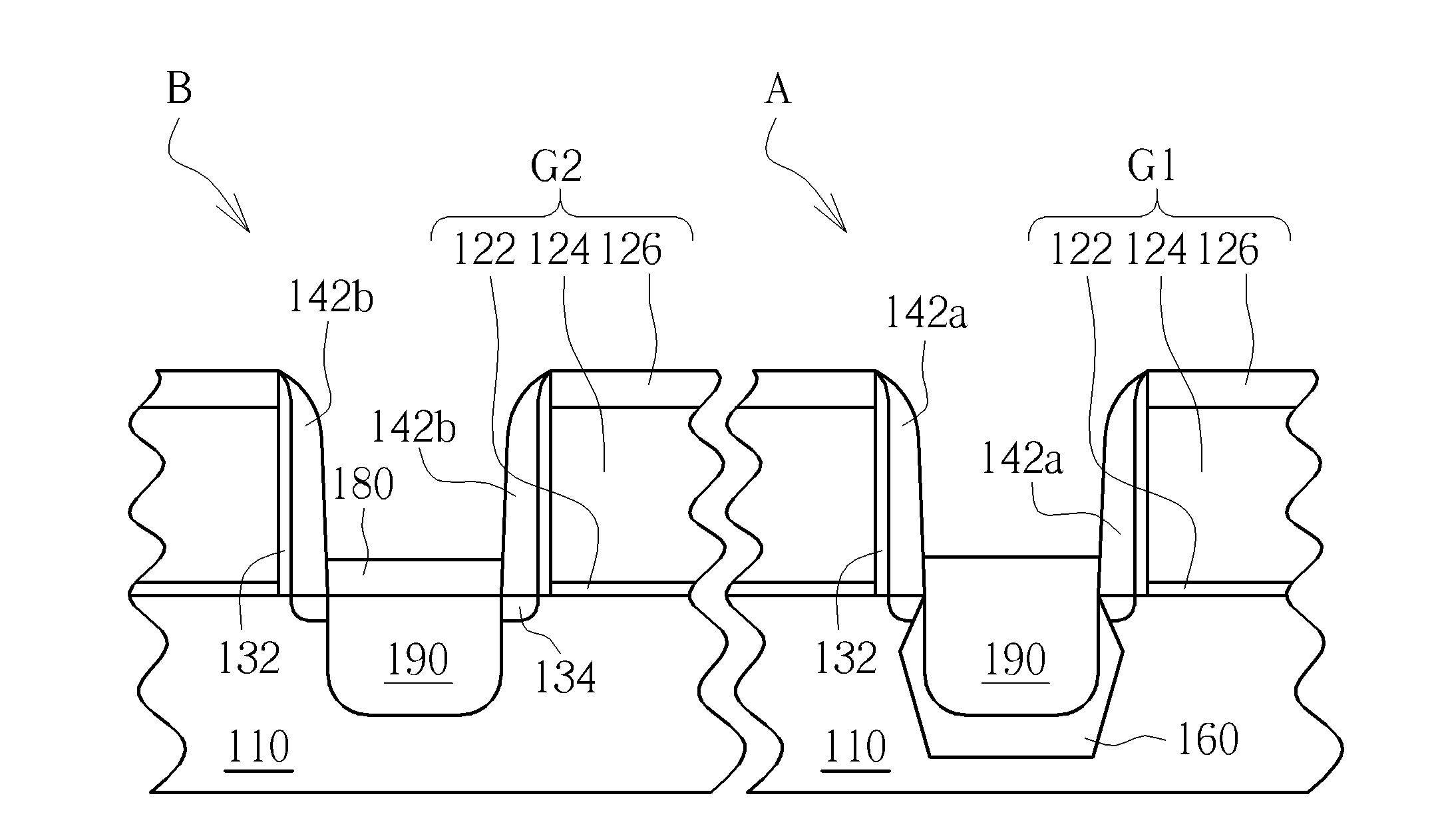
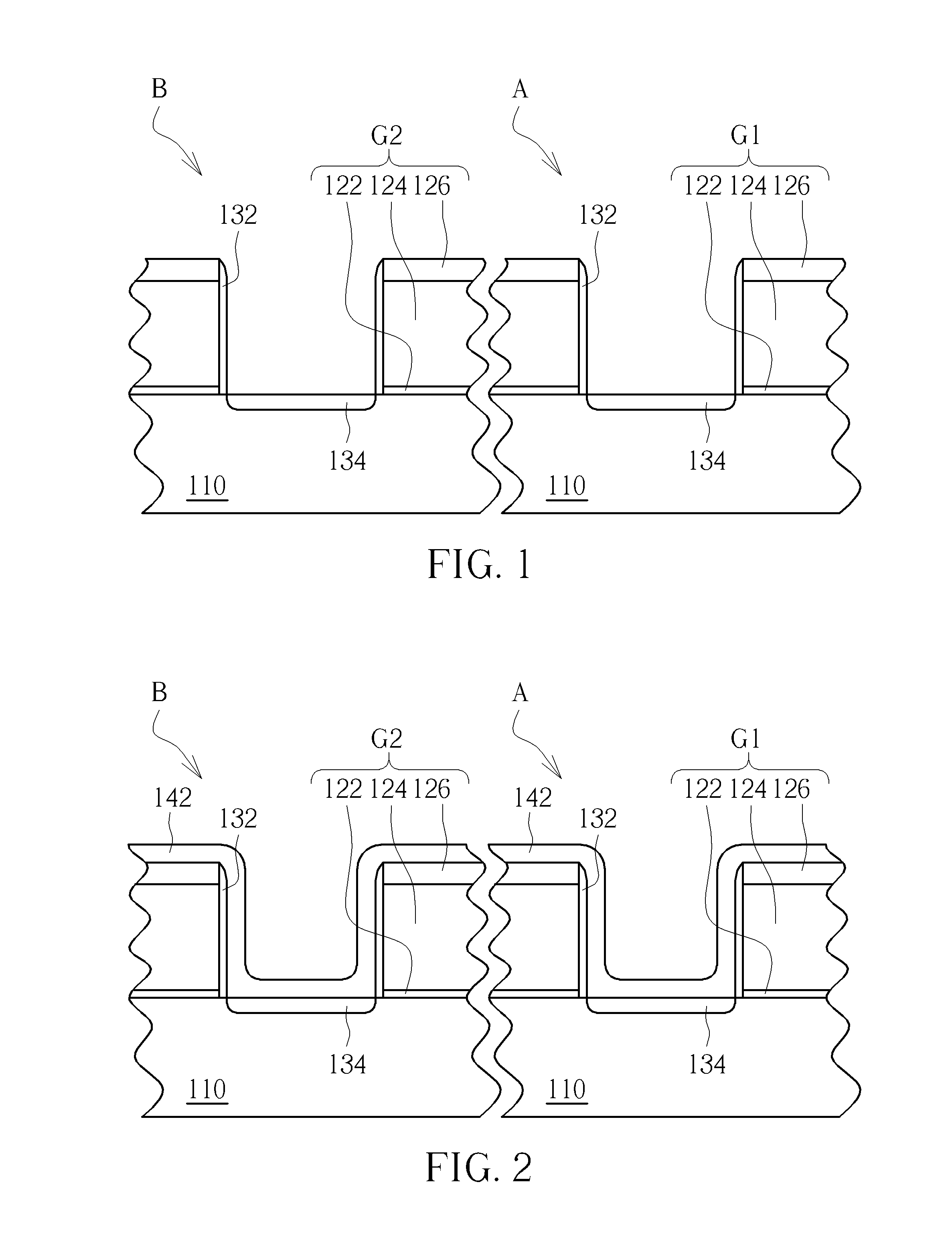
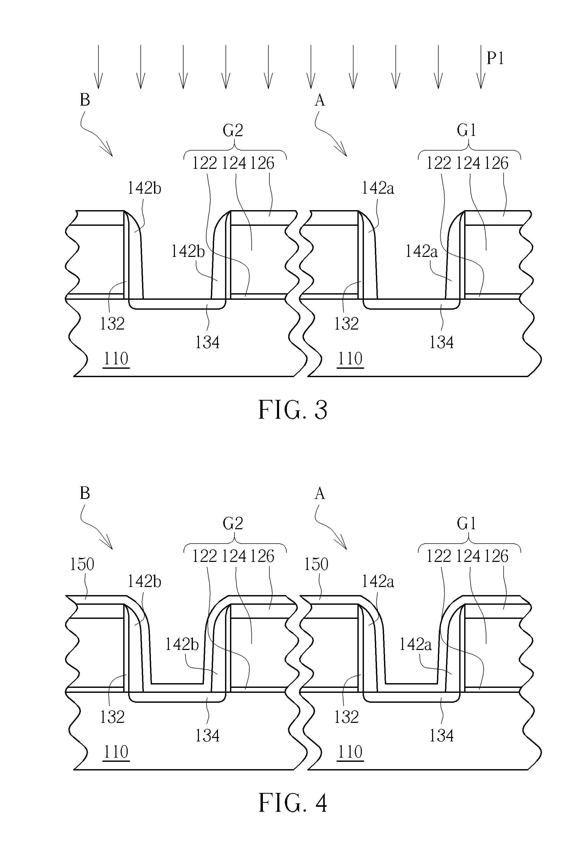
[0011]FIGS. 1-11 schematically depict cross-sectional views of an epitaxial process according to an embodiment of the present invention. A gate-last for high-K last process is applied in this embodiment, but the present invention can also use a gate-last for high-K first process, a gate-first process or a polysilicon gate process etc.
[0012]As shown in FIG. 1, a substrate 110 is provided. The substrate 110 may be a semiconductor substrate such as a silicon substrate, a silicon containing substrate, a III-V group-on-silicon (such as GaN-on-silicon) substrate, a graphene-on-silicon substrate or a silicon-on-insulator (SOI) substrate. The substrate 110 includes a first area A and a second area B. In this embodiment, the first area A is a PMOS transistor area and the second area B is an NMOS transistor area, but not limited thereto. In this embodiment, two first gates G1 and two second gates G2 are respectively formed in the first area A and the second area B, wherein each of the first g...
PUM
 Abstract
Description
Claims
Application Information
 - R&D
- Intellectual Property
- Life Sciences
- Materials
- Tech Scout
- Unparalleled Data Quality
- Higher Quality Content
- 60% Fewer Hallucinations
Browse by: Latest US Patents, China's latest patents, Technical Efficacy Thesaurus, Application Domain, Technology Topic, Popular Technical Reports.
© 2025 PatSnap. All rights reserved.Legal|Privacy policy|Modern Slavery Act Transparency Statement|Sitemap|About US| Contact US: help@patsnap.com