Wireless communication device

a wireless communication and wireless technology, applied in the field of wireless communication devices, can solve the problems of inability to efficiently use antenna efficiency, difficult to embed the lc resonant circuit in a small wireless communication device such as a mobile terminal, and inability to secure the necessary communication distance with a small antenna

Active Publication Date: 2014-08-21
MURATA MFG CO LTD
View PDF6 Cites 84 Cited by
  • Summary
  • Abstract
  • Description
  • Claims
  • Application Information

AI Technical Summary

Benefits of technology

[0014]With this configuration, the Q value of the antenna circuit is easily changed to many levels by using only a small number of IO terminals.

Problems solved by technology

Thus, it is difficult to embed the LC resonant circuits in a small wireless communication device such as a mobile terminal.
In addition, if an antenna with wide-band characteristics is simply used, the antenna efficiency cannot be efficiently used at the time of low-speed communication, and it is impossible to secure a necessary communication distance with a small antenna.

Method used


Image

  • Wireless communication device
  • Wireless communication device
  • Wireless communication device

Examples


first preferred embodiment

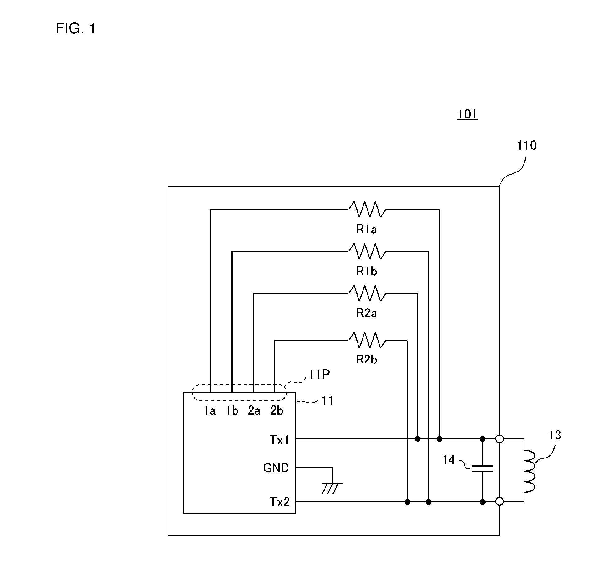
[0032]FIG. 1 is a circuit diagram of main portions of a wireless communication device 101 according to a first preferred embodiment of the present invention. The wireless communication device 101 includes a resistive-element-including RFIC 110 and an antenna coil 13. The resistive-element-including RFIC 110 includes an RFIC (a contactless communication IC) 11, a capacitive element 14, and resistive elements R1a, R1b, R2a, and R2b. The resistive elements R1a, R1b, R2a, and R2b and a portion of a circuit in the RFIC 11 configure a variable impedance circuit.

[0033]The RFIC 11 includes GPIO (General Purpose Input / Output) IO terminals 11P (1a, 1b, 2a, and 2b).

[0034]The RFIC 11 performs conversion between a baseband signal and a high-frequency signal. A control IC and the like are connected to the RFIC 11.

[0035]A parallel circuit of the capacitive element 14 and the antenna coil 13 is connected to two TX terminals (transmission signal terminals) Tx1 and Tx2 of the RFIC 11. Note that, alth...

second preferred embodiment

[0048]FIG. 6 is a circuit diagram of a wireless communication device 102 according to a second preferred embodiment of the present invention. The wireless communication device 102 is an example of an NFC module. The wireless communication device 102 includes a resistive-element-including RFIC 111, a control IC 12, and the antenna coil 13. The resistive-element-including RFIC 111 includes the RFIC (a contactless communication IC) 11, the capacitive element 14, the resistive elements R1a, R1b, R2a, and R2b, and switches SW1, SW2, SW3, and SW4. The resistive elements R1a, R1b, R2a, and R2b and the switches SW1, SW2, SW3, and SW4 configure a variable impedance circuit.

[0049]The RFIC 11 includes the GPIO (General Purpose Input / Output) IO terminals 11P (P1, P2, P3, and P4). The states of the switches SW1, SW2, SW3, and SW4 are changed in accordance with the output levels of these IO terminals. First ends of the resistive elements R1a, R1b, R2a, and R2b are connected to a first end of the ...

third preferred embodiment

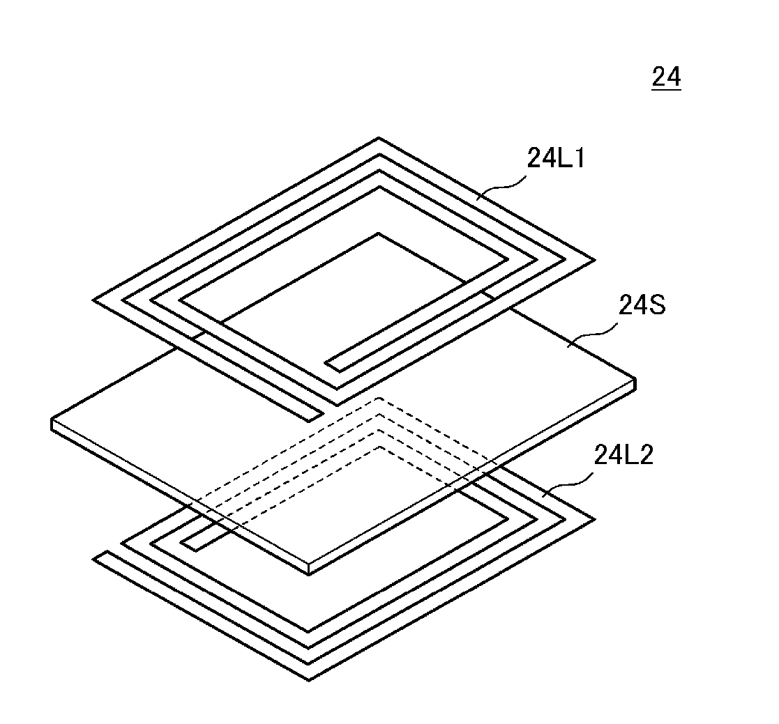
[0057]FIG. 7 is a diagram illustrating the configuration of the interior of a casing of a wireless communication device 103 according to a third preferred embodiment of the present invention, which is a plan view in a state in which a lower casing 51 and a upper casing 52 are separated to expose the interior. The interior of the lower casing 51 accommodates printed-wiring boards 21 and 31, a battery pack 33, and the like. The RFIC 11 and the resistive elements R1a, R1b, R2a, and R2b are mounted on the printed-wiring board 21. A UFH-band antenna 22, a camera module 26, and the like are also mounted on the printed-wiring board 21. In addition, a UFH-band antenna 32 and the like are mounted on the printed-wiring board 31. The printed-wiring board 21 and the printed-wiring board 31 are connected via a coaxial cable 34.

[0058]The antenna coil 13 is provided in the interior of the upper casing 52. The antenna coil 13 preferably is a conductor patterned in a rectangular or substantially rec...


PUM


Abstract

A wireless communication device includes a resistive-element-including RFIC and an antenna coil. The resistive-element-including RFIC includes an RFIC, a capacitive element, and resistive elements. The resistive elements and a portion of a circuit in the RFIC define a variable impedance circuit. The RFIC controls the impedance of a resistive circuit added to an antenna circuit in accordance with certain IO terminals set as output ports or input ports, thus obtaining a Q value of the antenna circuit in accordance with a communication speed.

Description

BACKGROUND OF THE INVENTION[0001]1. Field of the Invention[0002]The present invention relates to a wireless communication device preferably for use in an RFID (Radio Frequency Identification) system or a near field communication (NFC) system that communicates with a partner device via an electromagnetic field signal.[0003]2. Description of the Related Art[0004]NFC is a wireless communication standard combining contactless identification technology and interconnection technology. Devices conforming to this standard use a frequency in the 13.56 MHz band and perform bidirectional communication at a short distance of about a few tens of cm. There are multiple communication speeds (106 kbps, 212 kbps, 424 kbps, and 848 kbps) in NFC systems. Therefore, a wide-band antenna is necessary in order to perform communication without waveform distortion even at the highest communication speed.[0005]A design technique for widening the band of an antenna includes, as described in Japanese Unexamine...

Claims


Application Information

Patent Timeline
Patent Type & Authority Applications(United States)
IPC IPC(8): H01Q1/50G06K7/10G06K19/07H01Q1/22
CPCH01Q1/50G06K19/0723G06K7/10009H01Q1/2208H01Q7/00H04B1/18H01Q1/2216H01Q23/00G06K7/10237G06K19/07749H04B5/0062H04B5/0075G06K19/07794H04B5/0056H04B5/0081H04B1/0458
Inventor YOSUI, KUNIAKI
Owner MURATA MFG CO LTD
Why Eureka
Try Eureka