Connector and signal transmission method using the same
- Summary
- Abstract
- Description
- Claims
- Application Information
AI Technical Summary
Benefits of technology
Problems solved by technology
Method used
Image
Examples
first embodiment
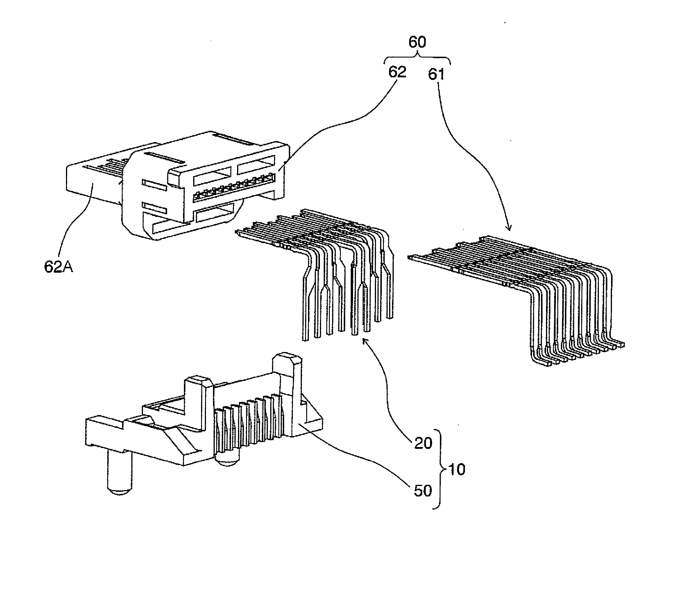
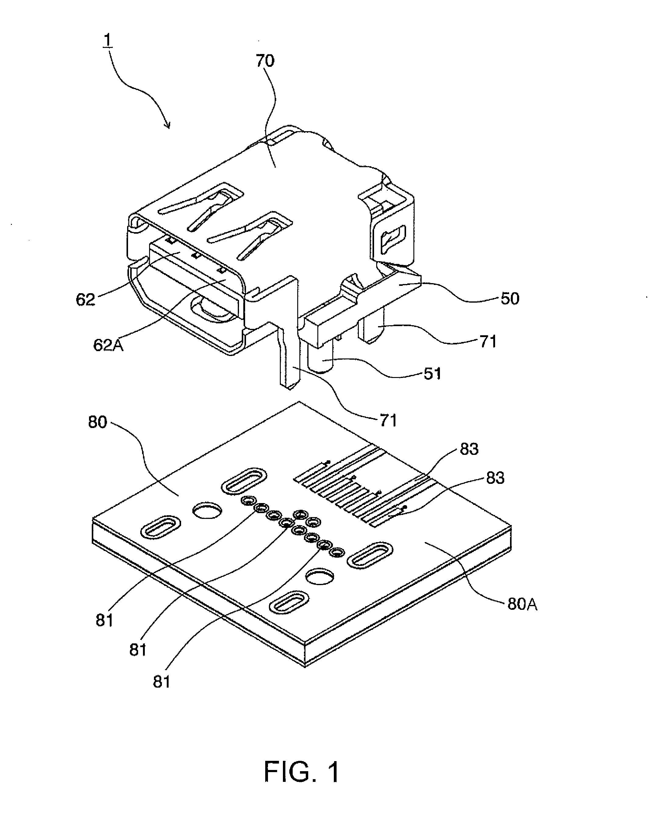
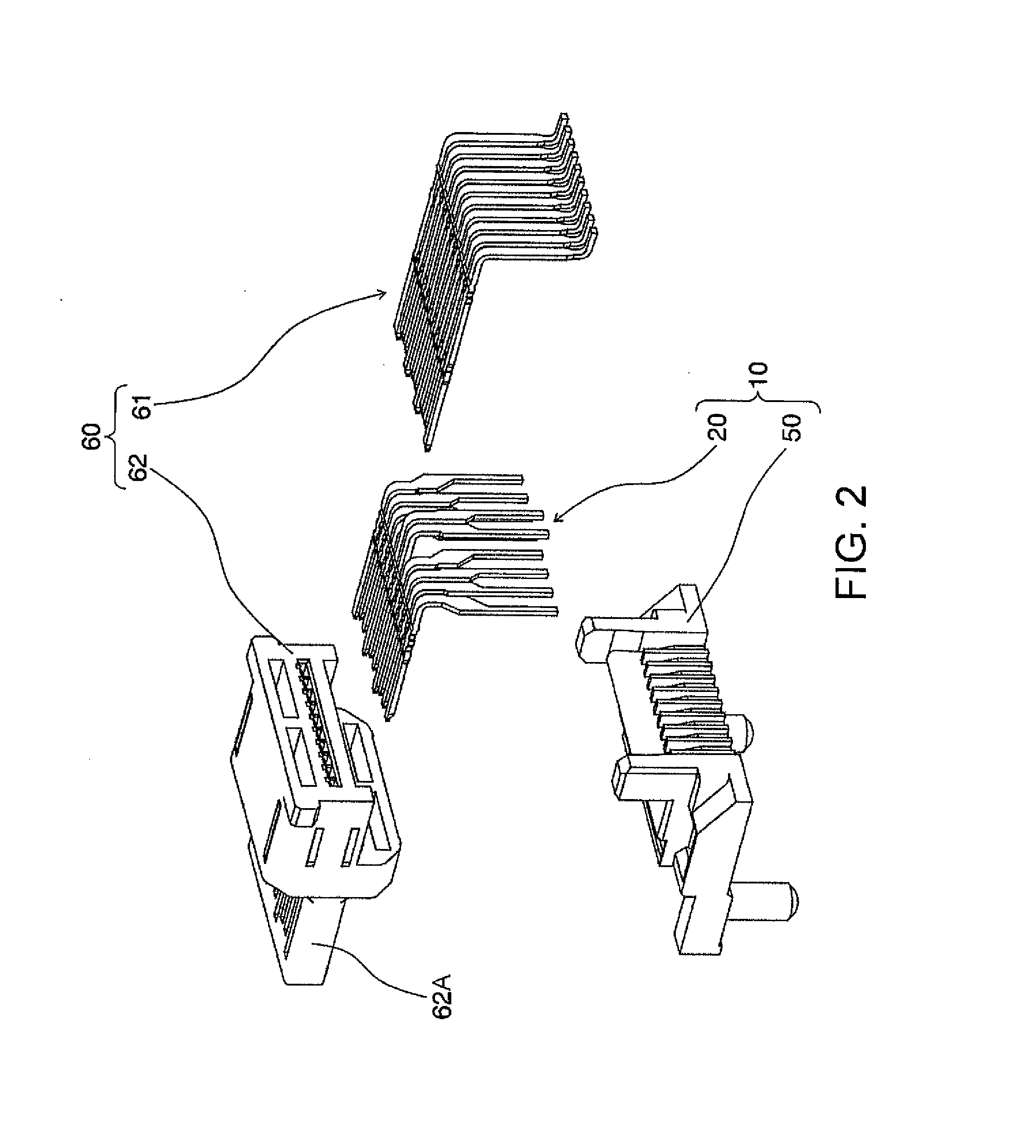
[0036]A connector 1 is a printed board mount connector adapted to be mounted to a printed board (mounting object) 80 and adapted to be fitted and connected to a mating connector (connecting object, not shown). In the following description, a front side of the connector 1 for connection with the mating connector (not shown) is called a first connection side while a bottom side of the connector 1 for connection with the printed board 80 is called a second connection side.
[0037]The printed board 80 used in this embodiment is a multilayer board. As shown in FIGS. 1 and 6, the printed board 80 is provided with a number of through holes 81. The printed board 80 has a lower surface 80B provided with a plurality of lands 82. Each of the lands 82 comprises a doughnut-shaped conductor pattern and is formed around an opening of each through hole 81. From some of the lands 82, a plurality of wiring patterns 84 are extracted along the printed board 80 in parallel to one another. Positions and f...
second embodiment
[0058]In this invention, the terminal portions 32B of the ground contacts 32 sandwiching the pair of the second contacts 40 and arranged on opposite sides of the pair of the second contacts 40 are combined with each other to form an integral structure, as shown in FIG. 7.
[0059]In the second embodiment described above, the two ground contacts 32 are combined into a single component. With this structure, the number of components is reduced. In addition, the number of the through holes 81 of the printed board 80 for insertion of the terminal portions 32B of the ground contacts 32 is reduced and the number of times of soldering during mounting of the connector 1 to the printed board 80 is reduced also. Thus, it is possible to reduce a load imposed during manufacture and mounting of the connector 1.
[0060]Next referring to FIG. 8, a third embodiment of this invention will be described. In the following, a difference from the first embodiment will only be described and components similar i...
third embodiment
[0061]In the third embodiment, the terminal portions 32B of the ground contacts 32 sandwiching the pair of the second contacts 40 and arranged on the opposite sides of the pair of the second contacts 40 are inserted into a common through hole 81 of the printed board 80, as shown in FIG. 8.
[0062]In the third embodiment described above, the number of the through holes 81 of the printed board 80 for insertion of the terminal portions 32B of the ground contacts 32 is reduced and the number of times of soldering during mounting of the connector 1 to the printed board 80 is reduced also. Thus, it is possible to reduce a load imposed during manufacture and mounting of the connector 1.
[0063]In the foregoing embodiments, description has been made about the case where the connector has two high-speed differential signal lanes each of which comprises the two first contacts and the two ground contacts. However, three or more high-speed differential signal lanes may be provided. In this event, t...
PUM
 Abstract
Description
Claims
Application Information
 - R&D
- Intellectual Property
- Life Sciences
- Materials
- Tech Scout
- Unparalleled Data Quality
- Higher Quality Content
- 60% Fewer Hallucinations
Browse by: Latest US Patents, China's latest patents, Technical Efficacy Thesaurus, Application Domain, Technology Topic, Popular Technical Reports.
© 2025 PatSnap. All rights reserved.Legal|Privacy policy|Modern Slavery Act Transparency Statement|Sitemap|About US| Contact US: help@patsnap.com


