Contact resistance reduction in finfets

a technology of contact resistance and finfets, applied in the field of semiconductor processing, can solve problems such as loss of performance, data errors, and increased heat and power loss

Inactive Publication Date: 2014-08-28
GLOBALFOUNDRIES INC +1
View PDF6 Cites 44 Cited by
  • Summary
  • Abstract
  • Description
  • Claims
  • Application Information

AI Technical Summary

Problems solved by technology

High contact resistance results in loss of performance, errors in data and increased heat and power loss, to name a few effects.
Smaller contact areas result in rapid increases in contact resistance.
With na...

Method used


Image

  • Contact resistance reduction in finfets
  • Contact resistance reduction in finfets
  • Contact resistance reduction in finfets

Examples


Embodiment Construction

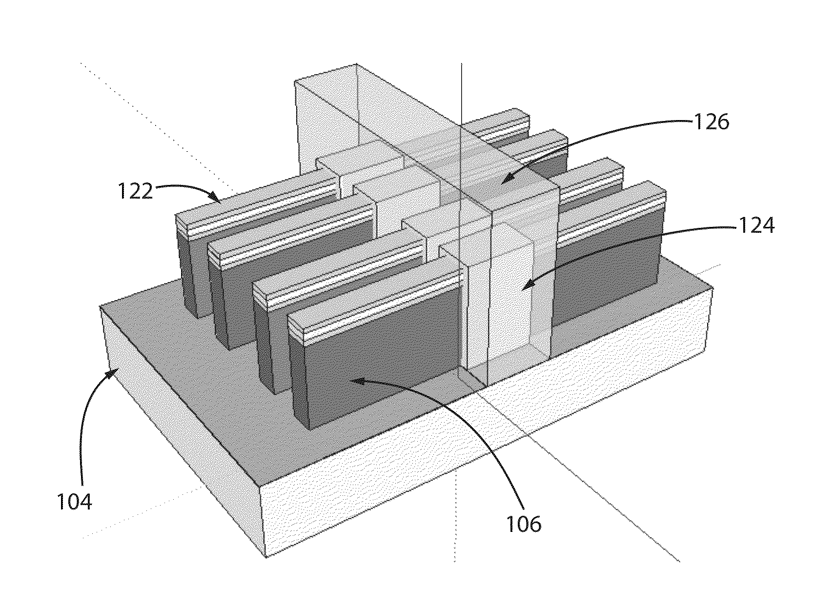
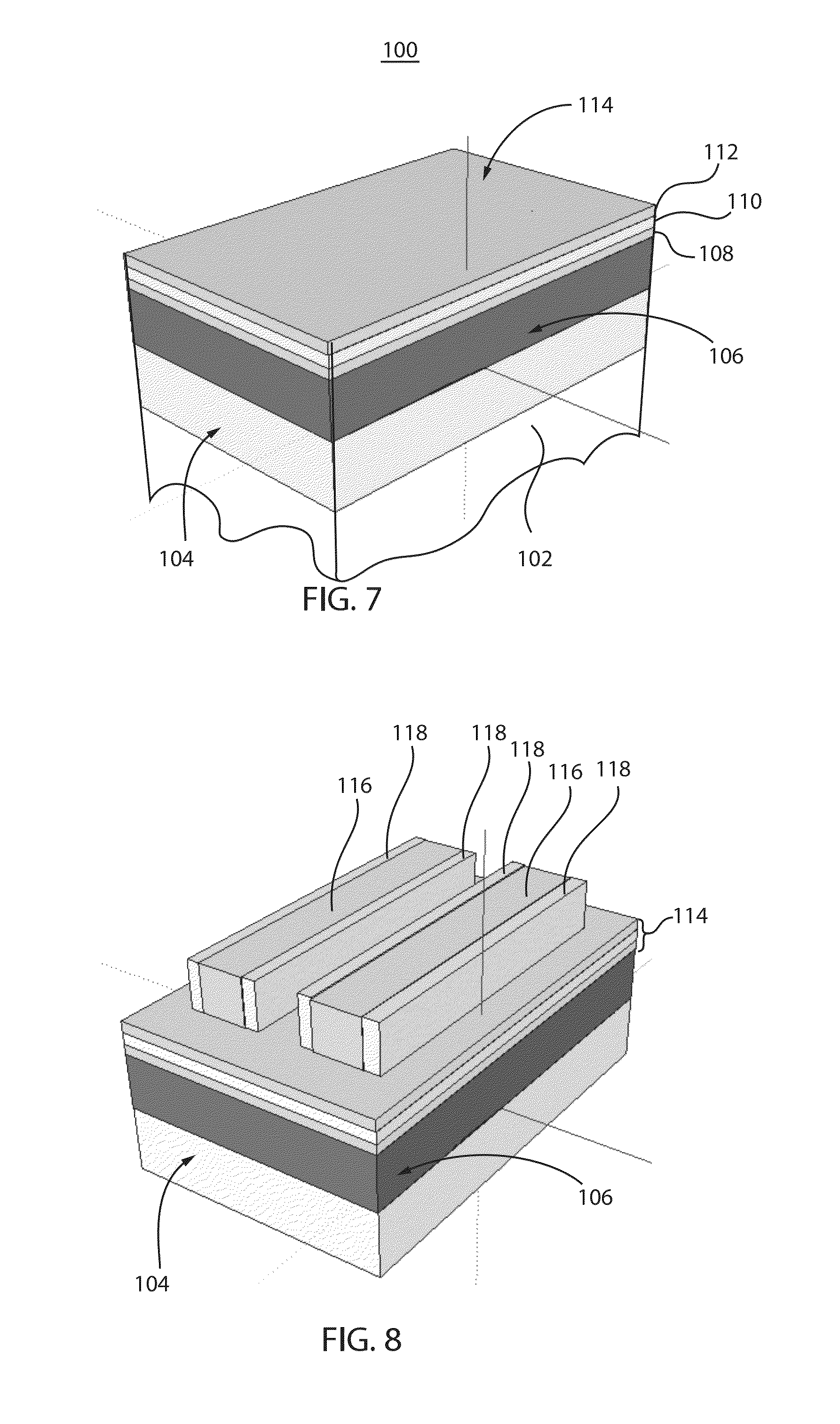
[0031]In accordance with the present principles, contact areas are increased by taking advantage of the surfaces provided by three-dimensional structures. In one particularly useful embodiment, the three-dimensional structures include fins formed in semiconductor material. Contact structures are formed in contact with the fins along with a higher conductivity material that is employed to wrap around the fin and make contact with the higher conductivity material. By increasing the effective area of the contact, contact resistance can be maintained or increased despite further reductions in pitch or device size.

[0032]The present aspects will be described in terms of fin structures employed for fin field effect transistors (finFETs); however, any three-dimensional structure may benefit from the decrease in contact resistance in accordance with the present principles.

[0033]It is to be understood that the present invention will be described in terms of a given illustrative architecture h...


PUM


Abstract

A method for forming contacts in a semiconductor device includes forming a plurality of substantially parallel semiconductor fins on a dielectric layer of a substrate having a gate structure formed transversely to a longitudinal axis of the fins. The fins are merged by epitaxially growing a crystalline material between the fins. A field dielectric layer is deposited over the fins and the crystalline material. Trenches that run transversely to the longitudinal axis of the fins are formed to expose the fins in the trenches. An interface layer is formed over portions of the fins exposed in the trenches. Contact lines are formed in the trenches that contact a top surface of the interface layer on the fins and at least a portion of side surfaces of the interface layer on the fins.

Description

BACKGROUND[0001]1. Technical Field[0002]The present invention relates to semiconductor processing, and more particularly to devices and methods for forming contacts for fin transistors with reduced contact resistance.[0003]2. Description of the Related Art[0004]High contact resistance results in loss of performance, errors in data and increased heat and power loss, to name a few effects. Contact resistance in semiconductor devices increases dramatically with reduction in pitch scaling sizes. Smaller contact areas result in rapid increases in contact resistance. With nanometer scale structures, such as fins for fin field effect transistors, smaller three-dimensional structures present particular difficulties in forming suitable contact areas to make adequate electrical contact.SUMMARY[0005]A method for forming contacts in a semiconductor device includes forming a plurality of substantially parallel semiconductor fins on a dielectric layer of a substrate having a gate structure formed...

Claims


Application Information

Patent Timeline
IPC IPC(8): H01L29/66H01L29/78
CPCH01L29/66795H01L29/785H01L29/66545H01L29/41791H01L29/165H01L29/456
Inventor BASKER, VEERARAGHAVAN S.LIU, QINGYAMASHITA, TENKOYEH, CHUN-CHEN
Owner GLOBALFOUNDRIES INC
Why Eureka
Try Eureka