Semiconductor device having compressively strained channel region and method of making same

a technology of compressively strained channel region and semiconductor device, which is applied in the direction of semiconductor device, electrical apparatus, basic electric element, etc., can solve the problem that the previous design effort will likely not meet the demands of future generations of semiconductor devi

Active Publication Date: 2014-08-28
RENESAS ELECTRONICS CORP
View PDF13 Cites 24 Cited by
  • Summary
  • Abstract
  • Description
  • Claims
  • Application Information

AI Technical Summary

Benefits of technology

[0014]In preferred embodiments of the semiconductor device according to the present invention, the second semiconductor material has a smaller lattice constant than the first semiconductor material, thereby to create a tensile strain in the epitaxial covering.

Problems solved by technology

However, previous design efforts will likely not meet the demands of future generations of semiconductor devices with respect to minimizing off-current while maximizing on-current and switching speed, especially as gate lengths decrease to 14 nm and below.

Method used


Image

  • Semiconductor device having compressively strained channel region and method of making same
  • Semiconductor device having compressively strained channel region and method of making same
  • Semiconductor device having compressively strained channel region and method of making same

Examples


Embodiment Construction

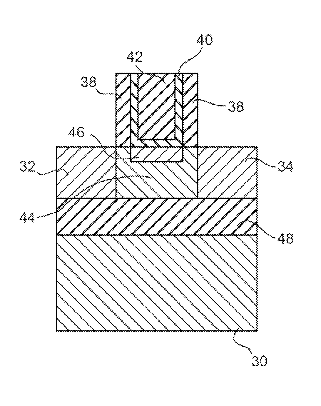
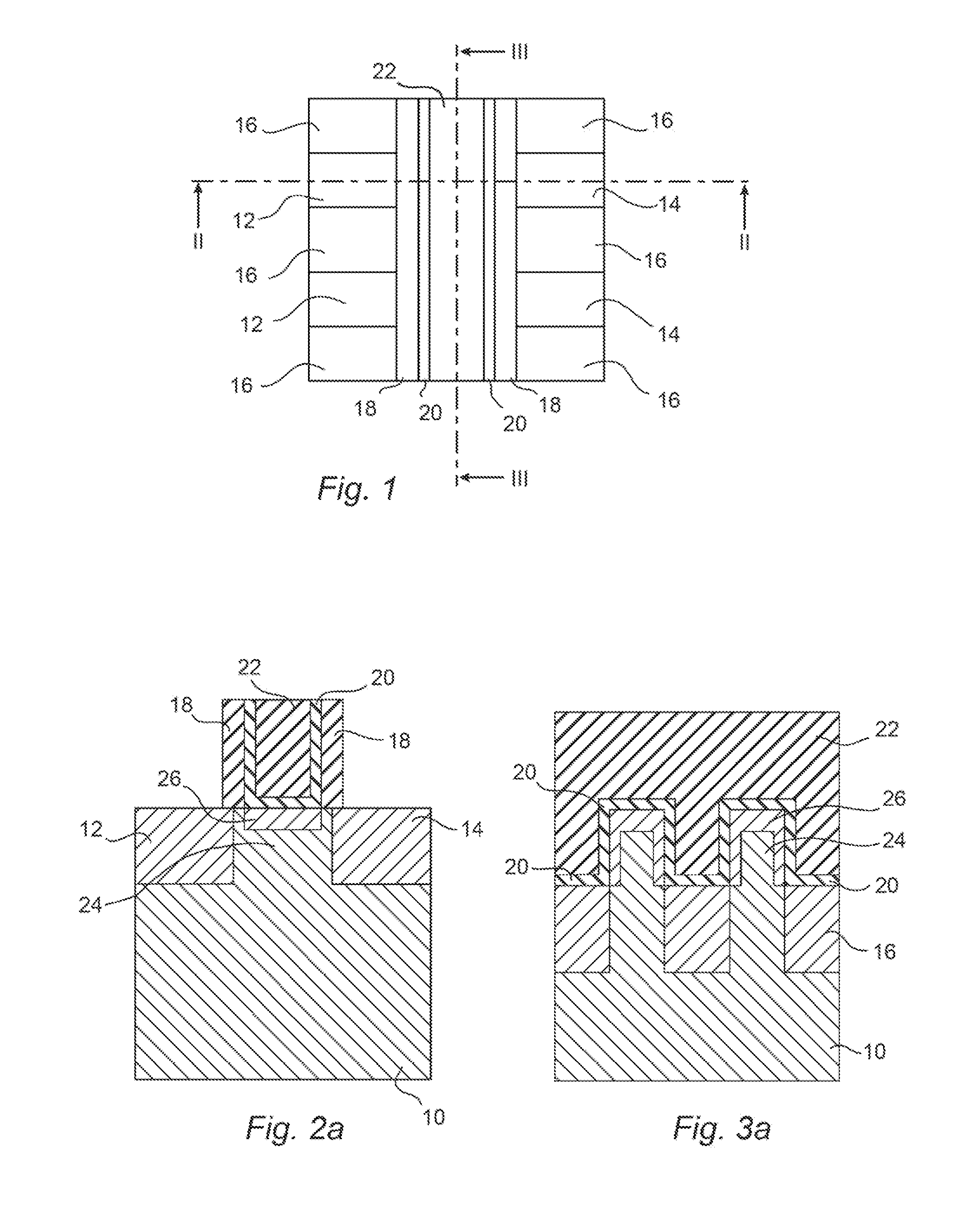
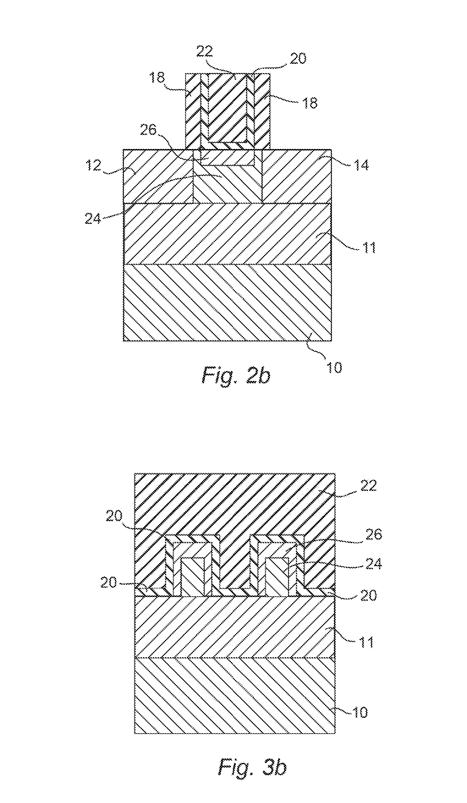
[0107]In FIGS. 1, 2a and 3a, a first embodiment of the present invention is a FinFET in which a series of silicon fins 24 has been formed integrally with an underlying bulk silicon substrate 10. A gate 22 extends across plural transistors as shown in FIG. 1, and is clad with a gate dielectric film 20. Source and drain regions of each transistor are designated 12 and 14, respectively.

[0108]A gate dielectric film 20 is positioned between the gate 22 and sidewall spacers 18, as shown in FIG. 2, and is also positioned between the gate electrode 22 and channel regions 26 as well as dielectric 16, as shown in FIGS. 2 and 3. The gate dielectric film 20 thus has a hollow, three-dimensional structure.

[0109]The upper part of Si fin 24 is clad with a layer of epitaxial silicon-germanium 26, as is best seen in FIGS. 2 and 3. As SiGe has a larger lattice constant than Si, the channel regions of the illustrated FinFET will be compressively strained. Although compressive strain is preferred for th...


PUM


Abstract

A semiconductor device and method making it utilize a three-dimensional channel region comprising a core of a first semiconductor material and an epitaxial covering of a second semiconductor material. The first and second semiconductor materials have respectively different lattice constants, thereby to create a strain in the epitaxial covering. The devices are formed by a gate-last process, so that the second semiconductor material is deposited only after the high temperature processes have been performed. Consequently, the lattice strain is not substantially relaxed, and the improved performance benefits of the lattice strained channel region are not compromised.

Description

BACKGROUND OF THE INVENTION[0001]1. Field of the Invention[0002]The invention relates to semiconductor devices and methods of making the same, and more particularly relates to such devices and methods in which a transistor channel region is compressively strained.[0003]2. Description of Related Art[0004]As the gate length of transistors continues to decrease with successive generations of semiconductor devices, new transistor configurations have been needed to counteract the diminished response that would otherwise occur with shrinking gate lengths. One such design configuration is referred to variously as a FinFET or tri-gate transistor, in which the source, drain and channel region of each transistor is elevated relative to a semiconductor substrate. The elevated portion has the shape of a ridge or fin, and may be formed integrally with the underlying substrate or may be formed on an insulating layer in the case of SOI type devices. The gate wraps around the three projecting sides...

Claims


Application Information

Patent Timeline
Patent Type & Authority Applications(United States)
IPC IPC(8): H01L29/78H01L29/66
CPCH01L29/785H01L29/66795H01L29/1054
Inventor NAGUMO, TOSHIHARU
Owner RENESAS ELECTRONICS CORP
Why Eureka
Try Eureka