Inspection probe and an IC socket with the same

a technology of ic socket and probe, which is applied in the direction of electrical testing, measurement devices, instruments, etc., can solve the problems of shortening the flow path by using the wound tight portion, and affecting the performance of the instrument. , to achieve the effect of stabilizing internal resistance, reducing the resistance value of the transmission path, and suitable for large-current us

Active Publication Date: 2014-09-11
YAMAICHI ELECTRONICS
View PDF10 Cites 22 Cited by
  • Summary
  • Abstract
  • Description
  • Claims
  • Application Information

AI Technical Summary

Benefits of technology

[0012]In view of the above-described mentioned problem, the present invention aims to provide an inspection probe and an IC socket with the same. The inspection probe and an IC socket with the same can reliably and stably reduce a resistance value of a transmission path to transmit an electric signal and avoid buckling of a spring portion, and are also suitable for large-current use.
[0018]According to the inspection probe of the present invention and the IC socket with the same, the inspection probe includes: the first plunger formed from a copper alloy material, and including the contact point configured to selectively come into contact with the electrode portion of the object to be inspected; the second plunger formed from the copper alloy material, and including the contact point configured to selectively come into contact with the electrode portion of the wiring board; the spring portion formed integrally with the one end of the first plunger and the one end of the second plunger, and configured to bias the first plunger and the second plunger in the direction away from each other; and the support stem formed into a cylindrical shape integrally with the other end of the second plunger in such a manner as to be disposed inside the spring portion with the predetermined clearance in between, and configured to slidably guide the spring portion. Thus, the inspection probe prevents the spring portion from bucking, reduces a resistance value of a transmission path to transmit an electric signal, and is suitable for large-current use. In addition, when the contact point of the first plunger comes into contact with the electrode portion of the object to be inspected, the one end of the support stem comes into sliding contact with the inner peripheral portion of the first plunger. This makes it possible to stabilize internal resistance, and thereby to reliably and stably reduce the resistance value of the transmission path.

Problems solved by technology

According to Japanese Patent Laid-Open No. 2010-157386, because the material of the coil spring unit used in the above-described inspection probe is most commonly a piano wire or a stainless steel wire to meet demands for load bearing and durability, there are limitations in improving the reduction in the resistance value of the coil spring unit by use of the plated membrane alone.
At that time, the work of subjecting the coil spring units to the relatively thickening plating may also develop a manufacturing problem that the coil spring units are apt to fix together in the plating process.
Moreover, the shortening of a flow path by use of the wound tight portion may be unstable and is not suitable for large-current use exceeding 3 (A) in particular.
In Japanese Patent Laid-Open No. 2006-266869, it is not easy to achieve proper positioning of the upper contact portion because the spring portion of the inspection probe has a strength problem that it is weak against a force in a direction orthogonal to the center axis of the inspection probe.
Moreover, when the spring portion is compressed, the spring portion may buckle significantly because the short-circuit piece does not coincide with the center axis of the spring portion.
Furthermore, since a lower end portion of the short-circuit piece is configured to come into contact with the lower contact portion at one point, this configuration is accompanied by problems of instabilities in internal contact, internal slide, and internal resistance value due to a change in contact load when the inspection probe is tilted.

Method used


Image

  • Inspection probe and an IC socket with the same
  • Inspection probe and an IC socket with the same
  • Inspection probe and an IC socket with the same

Examples


Embodiment Construction

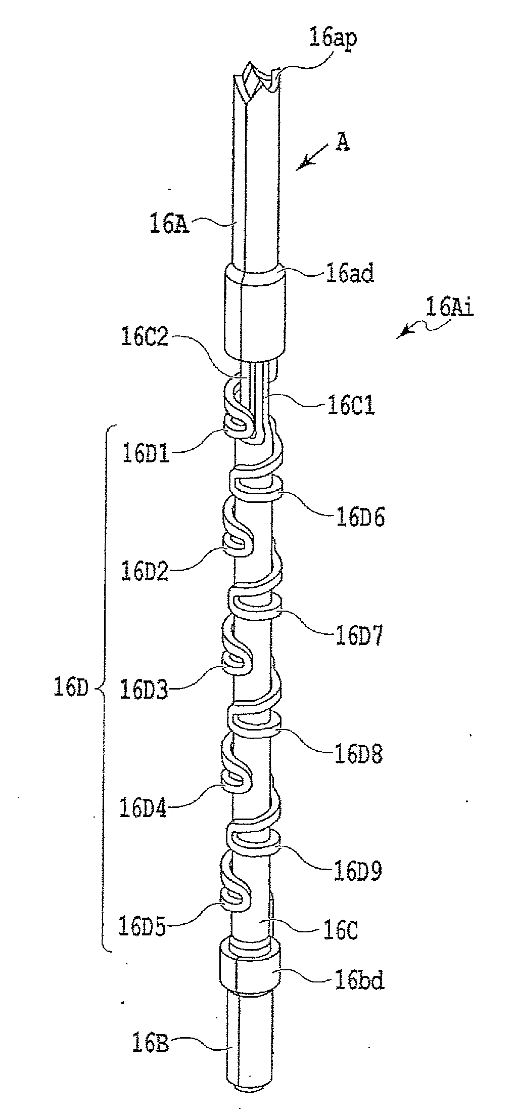
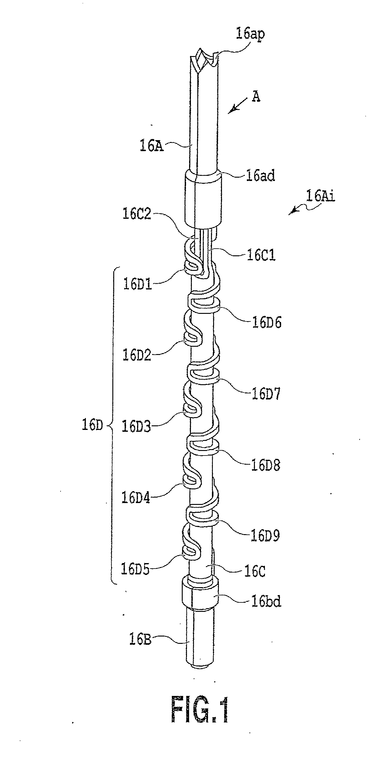
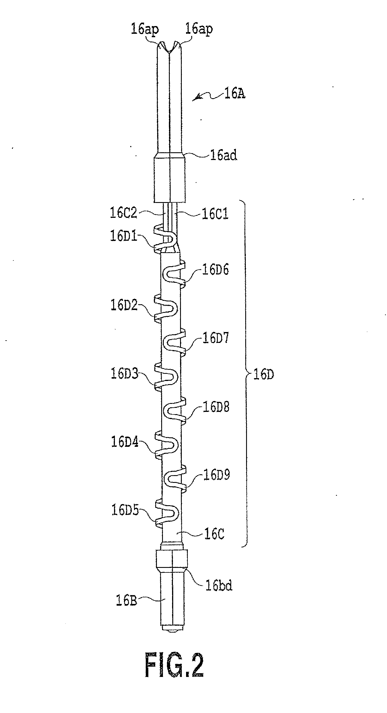
[0030]FIG. 3 schematically shows a configuration of an example of an IC socket according to the present invention.

[0031]In FIG. 3, a plurality of IC sockets are disposed on a mounting surface of a given printed wiring board 18. Note that FIG. 3 typically illustrates one of the IC sockets. The IC socket is configured to electrically connect contact pads formed on the mounting surface of the printed wiring board (a test board) 18 to electrode portions DVb of a semiconductor device DV which is to be attached as an object to be inspected. The semiconductor device DV is provided with an integrated circuit disposed in a BGA (Ball Grid Array) package, for example. The multiple electrode portions DVb (see FIG. 3 and FIG. 4C) are formed in a matrix on a bottom portion of the semiconductor device DV. Note that the semiconductor device is not limited only to the BGA packaged device but may also be an LGA (Land Grid Array) packaged device, for instance.

[0032]The printed wiring board 18 is made ...


PUM


Abstract

An inspection probe 16Ai is formed by subjecting a thin sheet material made of a copper alloy to press working. The inspection probe 16Ai includes: a device side plunger 16A having a contact point which selectively comes into contact with an electrode portion DVb of a semiconductor device DV; a board side plunger 16B having a contact point which selectively comes into contact with a contact pad of a printed wiring board 18; a spring portion 16D which biases the device side plunger 16A and the board side plunger 16B in a direction away from each other; and a cylindrical support stem 16C being disposed inside the spring portion 16D, making the spring portion 16D slidable thereon, and being configured to retain straight advancing property of the spring portion 16D.

Description

CROSS-REFERENCES TO RELATED APPLICATIONS[0001]This application claims the benefit of Japanese Patent Application No. 2013-040819, filed Mar. 1, 2013, which is hereby incorporated by reference herein in its entirety.BACKGROUND OF THE INVENTION[0002]1. Field of the Invention[0003]The present invention relates to an inspection probe and an IC socket with the same.[0004]2. Description of the Related Art[0005]On a semiconductor device serving as an electronic device to be mounted on electronic equipment or the like, a test for eliminating a potential failure is generally performed by use of a semiconductor device socket at a stage before the device is mounted. The semiconductor device socket used for the test or the mounting is generally referred to as an IC socket (integrated circuit socket), which is disposed on a printed wiring board (a test board or a mounting board) as disclosed in Japanese Patent Laid-Open No. 2010-157386, for example. In the IC socket, a plurality of inspection pr...

Claims


Application Information

Patent Timeline
Patent Type & Authority Applications(United States)
IPC IPC(8): G01R1/073G01R1/067
CPCG01R1/06733G01R1/06722
Inventor SUZUKI, KATSUMINAKAMURA, YUJISUZUKI, TAKEYUKIOTA, YUKIO
Owner YAMAICHI ELECTRONICS
Why Eureka
Try Eureka