Touch unit array and a display panel having the same

a display panel and touch unit technology, applied in the field of touch unit arrays, can solve the problems of inability of capacitance devices to sensing touch signals, inability to detect the decrease in capacitance between electrodes around the touched spot, etc., and achieve the effect of strong touch sensing sensitivity of self-capacitance devices and effective detection

Active Publication Date: 2014-09-11
AU OPTRONICS CORP
View PDF8 Cites 92 Cited by
  • Summary
  • Abstract
  • Description
  • Claims
  • Application Information

AI Technical Summary

Benefits of technology

[0070]In the touch unit array 800, the first electrode pad 102a of the first strip electrode 102 and the second electrode pad 104a of the second strip electrode 104 are the mutual capacitance device of the sixth embodiment. That is, the first electrode pad 102a and the second electrode pad 104a adjacent to the first electrode pad 102a are one pair of mutual capacitance electrodes. On the other hand, the electrode pad unit 806 is the self capacitance device of the sixth embodiment. Each first strip electrode 102 receives a second driving signal therefore each first electrode pad 102a of each first strip electrode 102 possesses a voltage. Each electrode pad unit 806 receives a first driving signal. The driving method and the principle of operation of the second embodiment are similar to those of the first embodiment, and therefore the details are omitted here. Comparing to the touch unit array 400 illustrated in FIG. 4, the density of the electrode pad unit 806 of the touch unit array 800 illustrated in FIG. 8 is one-second of the density of the electrode pad unit 106 of the touch unit array 400, therefore the precision of sensing locations of the touch unit array 800 may be not as precise as the touch unit array 400. However, since the electrode pad unit 806 includes two electrode pads 106a, the intensity of the touch sensing of the electrode pad unit 806 is still stronger than that of the electrode pad unit 106. The intensity of the touch sensing of the electrode pad unit increases when the electrode pad unit includes more electrode pads 106a. Therefore, the touch unit array 800 has stronger touch sensing sensitivity of the self capacitance devices. Although the quantity of the electrode pad unit 806 is fewer than that of the electrode pad unit 106, the intensity of the touch sensing of each electrode pad unit 806 is stronger than that of each electrode pad unit 106. Accordingly, the issue of short detecting distance of the mutual capacitance devices can be compensated, and the sensing signals can be effectively detected when the touching object is relatively distant from the touch unit array 800.

Problems solved by technology

However, as aforementioned, the mutual capacitance devices may not be capable of sensing the touch signal when the touching object is relatively distant from the touch unit array.
As such, the decrease in capacitance between the electrodes around the touched spot may not be detected when the touching object is not close enough to the touch unit array.

Method used


Image

  • Touch unit array and a display panel having the same
  • Touch unit array and a display panel having the same
  • Touch unit array and a display panel having the same

Examples


first embodiment

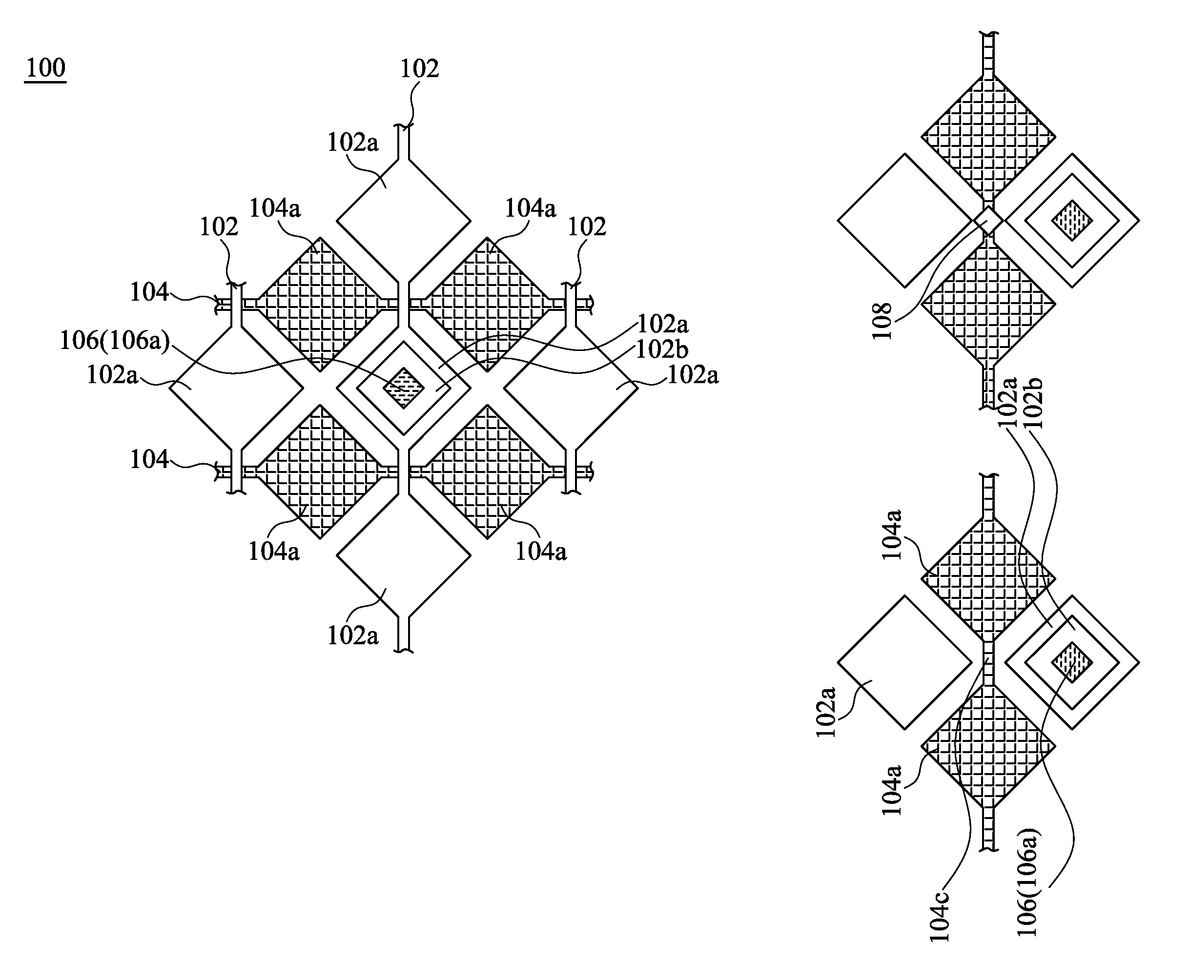
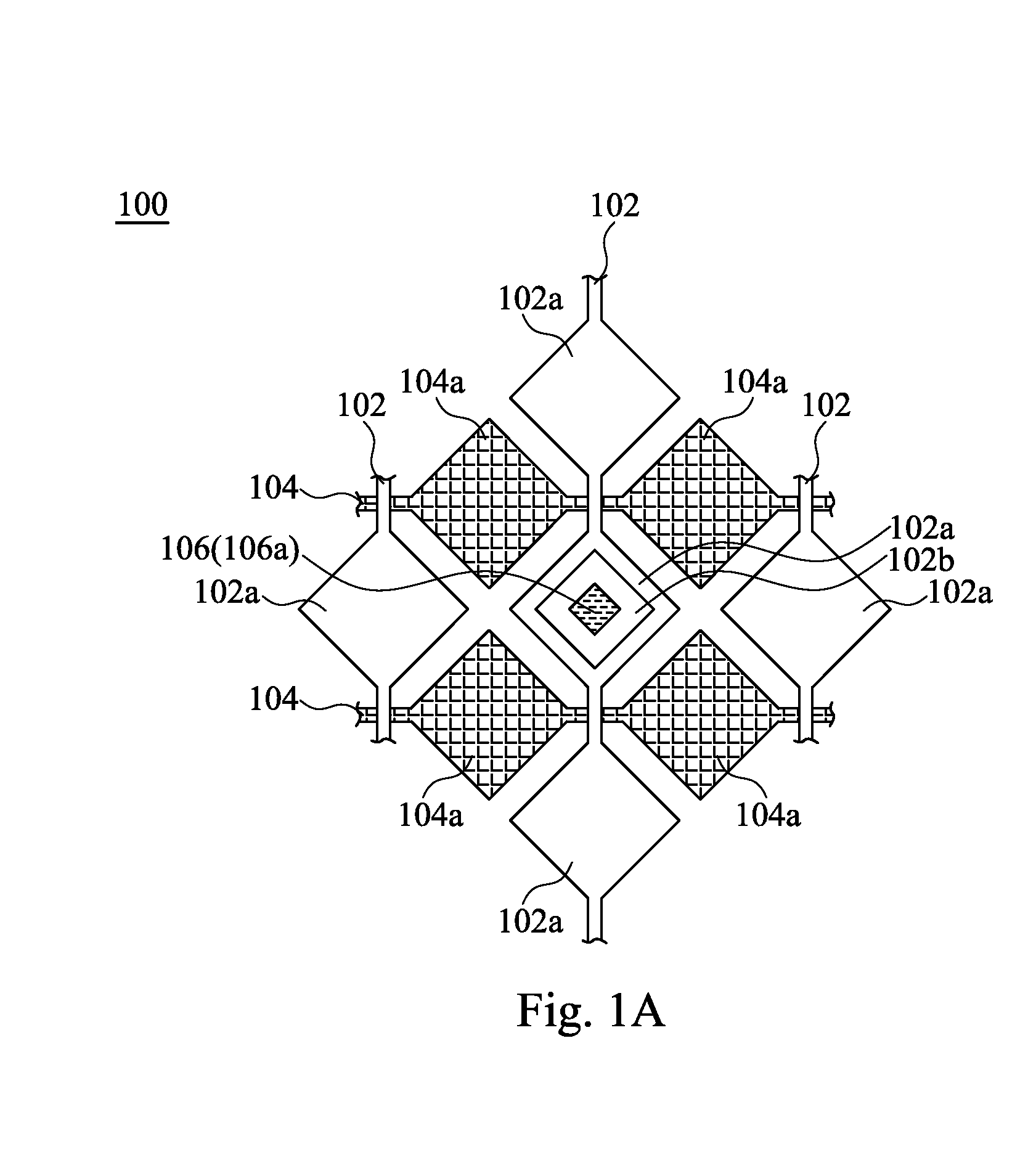
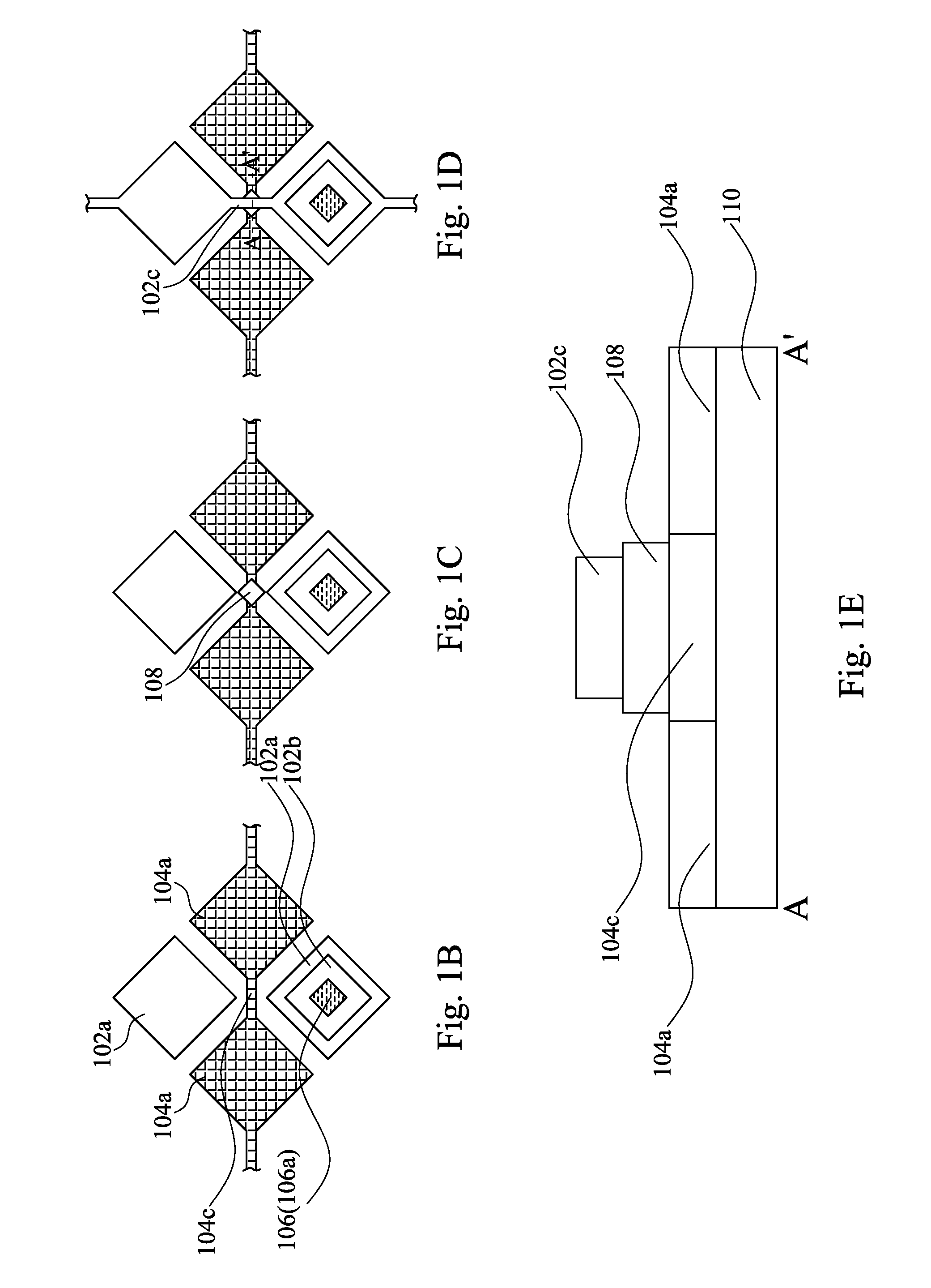
[0057]Referring to FIG. 1A, FIG. 1A is a schematic view of a portion of a touch unit array 100 according to the present disclosure. The touch unit array 100 includes a plurality of first strip electrodes 102, a plurality of second strip electrodes 104, and a plurality of electrode pad units 106. The first strip electrodes 102 and the second strip electrodes 104 are interlaced and electrically isolated with each other. The extending direction of the first strip electrodes 102 may be orthogonal to that of the second strip electrodes 104, however, the present disclosure is not limited thereto. As illustrated in FIG. 1A, each first strip electrode 102 includes a plurality of electrically connected first electrode pads 102a, and each second strip electrode 104 includes a plurality of electrically connected second electrode pads 104a, wherein at least one first electrode pad 102a has a first opening 102b. The fabricating sequence of each first strip electrode 102 and each second strip ele...

fifth embodiment

[0068]Referring to FIG. 5 and FIG. 7B, the plurality of electrode pad units 506 is shown in FIG. 7B. In the touch unit array 500 according to the present disclosure, each electrode pad unit 506 includes four adjacent and mutually electrically connected electrode pads 106a. Each electrode pad unit 506 receives a first driving signal. The first driving signal may be a waveform signal. For example, the waveform signal may be a sine wave, a cosine wave, a square wave, a triangular wave, or a sawtooth wave. However, the present disclosure is not limited thereto. In summary, the touch unit array 500 is a touch unit array integrated both mutual capacitance devices and self capacitance devices. Accordingly, the touch unit array 500 is capable to utilize both touch sensing devices with different sensing methods. By the coping with both mutual capacitance devices and self capacitance devices, the touch sensing signals generated by the touching object can be detected regardless the touching ob...


PUM


Abstract

A touch unit array including a plurality of first strip electrodes, a plurality of second strip electrodes, and a plurality of electrode pad units is provided. Each first strip electrode has at least one first opening. The second strip electrodes are orthogonally arranged to the plurality of first strip electrodes. Each electrode pad unit includes at least one electrode pad, and the electrode pads are respectively disposed in the plurality of first openings, wherein each electrode pad unit receives a first driving signal.

Description

RELATED APPLICATIONS[0001]This application claims priority to Taiwan Application Serial Number 102108076, filed Mar. 7, 2013, which is herein incorporated by reference.BACKGROUND[0002]1. Technical Field[0003]The present disclosure relates to a touch unit array, and more particularly, to a touch unit array with integrated touch technologies.[0004]2. Description of Related Art[0005]Capacitive touch unit array is an inputting device by utilizing electrons from a touching object, e.g. a finger, to input data. When the touching object touches or slides over a spot of the touch unit array, the capacitance of the spot of the touch unit array varies accordingly. By detecting the signals generated from the variation of the capacitance, the touched spot can be located. Capacitive touch unit array is applied in a variety of electronic products because of the thin thickness. The capacitive devices in the touch unit array can be classified as mutual capacitance devices and self capacitance devic...

Claims


Application Information

Patent Timeline
Patent Type & Authority Applications(United States)
IPC IPC(8): G06F3/044
CPCG06F3/044G06F3/0445G06F3/0446G06F3/0448G06F2203/04103G06F2203/04111
Inventor LEE, CHIA-CHICHENG, WEI-JOUWENG, YO-FUHSU, CHE-CHIALU, YING-CHILEE, SEOK-LYUL
Owner AU OPTRONICS CORP
Why Eureka
Try Eureka