Semiconductor optical waveguide device and method for manufacturing the same

Active Publication Date: 2014-09-11
SUMITOMO ELECTRIC IND LTD
View PDF0 Cites 9 Cited by
  • Summary
  • Abstract
  • Description
  • Claims
  • Application Information

AI Technical Summary

Benefits of technology

[0022]In the semiconductor optical waveguide device, the first mesa portion of the second semiconductor mesa includes the first portion (having a smaller width than the second mesa portion of the second semiconductor mesa) and the second portion (a tape

Problems solved by technology

This difference causes an optical coupling loss between t

Method used


Image

  • Semiconductor optical waveguide device and method for manufacturing the same
  • Semiconductor optical waveguide device and method for manufacturing the same
  • Semiconductor optical waveguide device and method for manufacturing the same

Examples


Example

[0071]The present invention will be better understood from the following detailed description with reference to the accompanying drawings. A semiconductor optical waveguide device and a method for manufacturing the semiconductor optical waveguide device according to an embodiment of the present invention will be described below with reference to the accompanying drawings. Like reference numerals designate like parts throughout these figures.

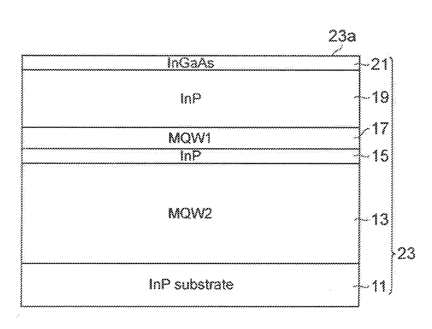
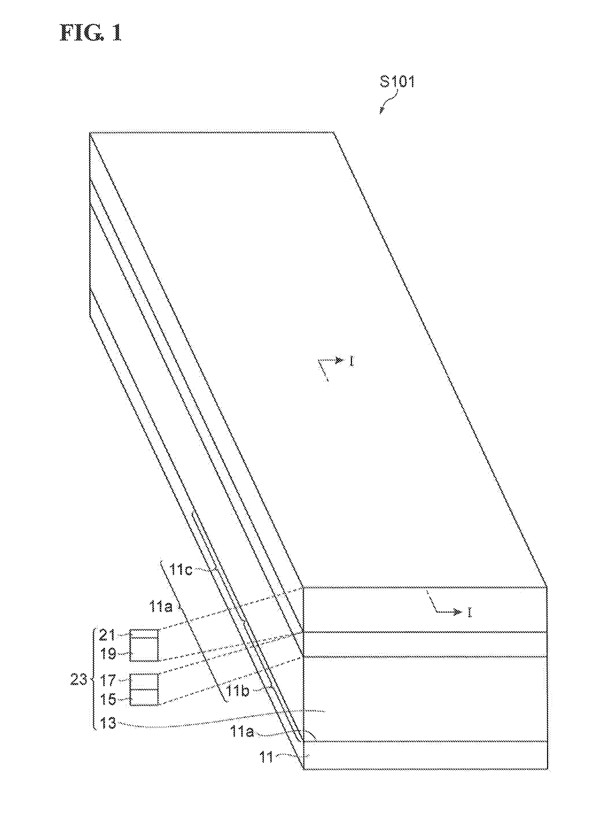
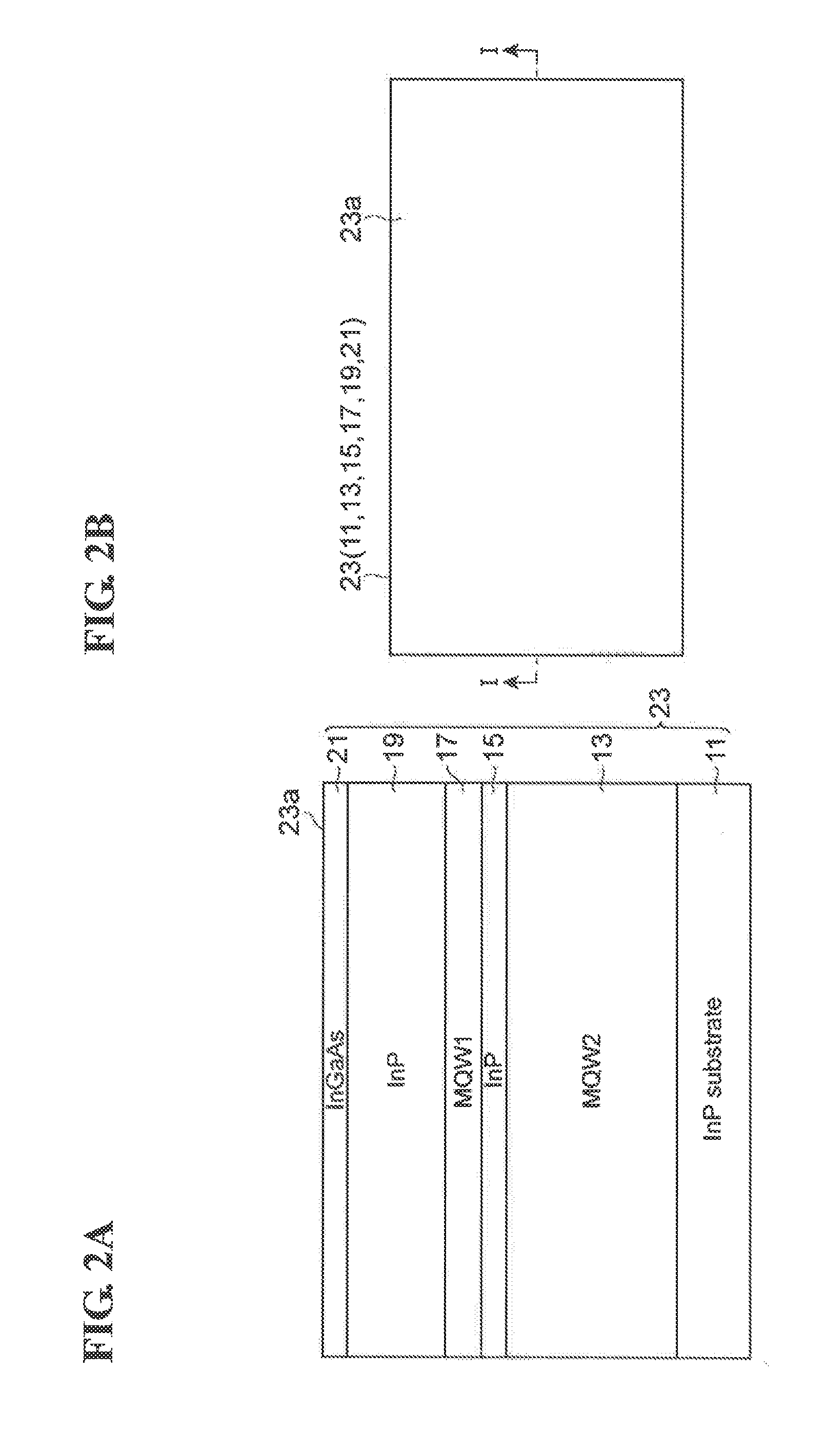
[0072]FIGS. 1 to 33C are schematic views of steps of a method for manufacturing a semiconductor optical waveguide device including a spot size converter according to an embodiment of the present invention. In step S101, as illustrated in FIG. 1, a substrate 11 on which a stacked semiconductor layer is grown is prepared. The substrate 11 is formed of a III-V group compound semiconductor and has a principal surface 11a. A second semiconductor layer 13 serving as a second core layer, a second III-V group compound semiconductor layer 15 serving as an...


PUM


Abstract

A semiconductor optical waveguide device includes a substrate having a first area and a second area, and first, second, and semiconductor mesas on the substrate. The first semiconductor mesa includes a cladding layer and a first mesa portion on the second area, the first mesa portion including first and second portions. The second semiconductor mesa includes an intermediate layer, a first core layer, and first and second mesa portions on the first and second area, respectively. The third semiconductor mesa includes a second core layer, and first and second mesa portions having a greater width than that of the second semiconductor mesa. The first portion of the first semiconductor mesa has a substantially the same width as the second mesa portion of the second semiconductor mesa. The first core layer is optically coupled to the second core layer through the intermediate layer disposed between the first and second core layers.

Description

BACKGROUND OF THE INVENTION[0001]1. Field of the Invention[0002]The present invention relates to a semiconductor optical waveguide device and a method for manufacturing the semiconductor optical waveguide device.[0003]2. Description of the Related Art[0004]U.S. Pat. No. 6,310,995 discloses an optical waveguide device including a spot size converter.[0005]III-V group compound semiconductors have a refractive index of 3 or more for light in a near-infrared wavelength band used in optical communication or optical information processing. In an optical waveguide formed of a III-V group compound semiconductor having such a high refractive index, optical propagation in a fundamental transverse mode through the optical waveguide requires an optical waveguide width of 2 or less. The half-width in a light distribution of a transverse mode confined in the optical waveguide is much less than 2 μm.[0006]The optical waveguide device such as a semiconductor optical modulator is optically coupled t...

Claims


Application Information

Patent Timeline
IPC IPC(8): G02B6/42G02B6/136
CPCG02B6/136G02B6/4201G02B6/1228G02B6/305G02B2006/12078G02F1/01708G02F1/2257G02F2201/04G02F2201/06G02F2201/063G02F2201/12G02F2202/101G02F2202/102G02F2202/108G02F1/212G02F1/217
Inventor FURUYA, AKIRAKITAMURA, TAKAMITSUYAGI, HIDEKIKONO, NAOYA
Owner SUMITOMO ELECTRIC IND LTD
Why Eureka
Try Eureka