Light-Emitting Element, Light-Emitting Device, Electronic Appliance, and Lighting Device

a technology of light-emitting devices and light-emitting elements, which is applied in the direction of thermoelectric device junction materials, semiconductor devices, electrical apparatus, etc., can solve the problems of increasing driving voltage or reliability, affecting the efficiency of light-emitting devices, etc., to achieve low driving voltage, improve productivity, and high emission efficiency

Active Publication Date: 2014-10-02
SEMICON ENERGY LAB CO LTD
View PDF7 Cites 33 Cited by
  • Summary
  • Abstract
  • Description
  • Claims
  • Application Information

AI Technical Summary

Benefits of technology

[0016]A light-emitting element which includes a plurality of light-emitting layers between a pair of electrodes and has low driving voltage and high emission efficiency can be provided as a light-emitting element of one embodiment present invention. Further, productivity can be improved at the time of forming the light-emitting element.

Problems solved by technology

Further, in the case of such a structure, the hole-transport layer or the electron-transport layer is shared by pixels emitting different colors; therefore, each pixel does not have an optimal structure, which causes a problem in that an abnormal state of the element characteristics, e.g., an increase in driving voltage or a reduction in reliability, occurs in at least one of the plurality of pixels.

Method used


Image

  • Light-Emitting Element, Light-Emitting Device, Electronic Appliance, and Lighting Device
  • Light-Emitting Element, Light-Emitting Device, Electronic Appliance, and Lighting Device
  • Light-Emitting Element, Light-Emitting Device, Electronic Appliance, and Lighting Device

Examples


embodiment 1

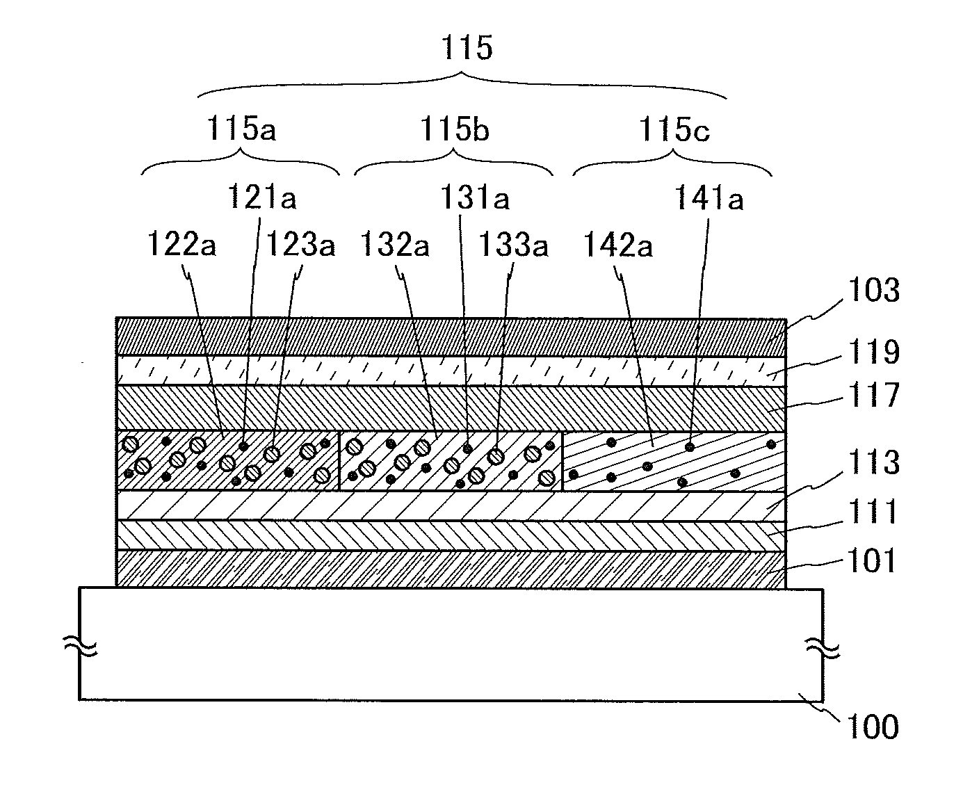
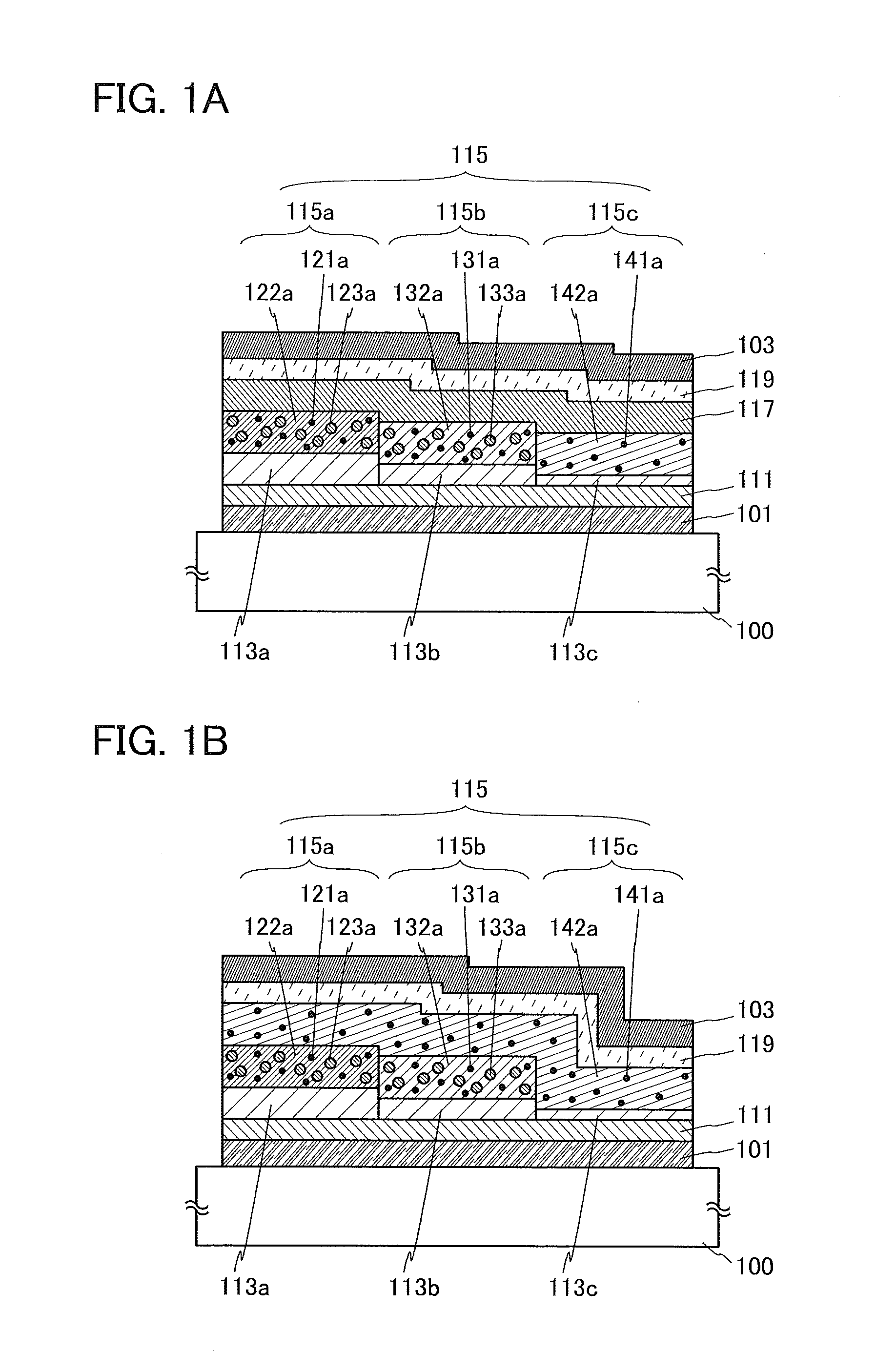
[0047]In this embodiment, a structural concept of a light-emitting element of one embodiment of the present invention and a specific structure of the light-emitting element are described. First, the light-emitting element that is one embodiment of the present invention is described with reference to FIGS. 1A and 1B.

[0048]A light-emitting element illustrated in FIG. 1A includes a light-emitting layer 115 between a pair of electrodes (an anode 101 and a cathode 103). The light-emitting layer 115 includes a first light-emitting layer 115a including a first phosphorescent material 121a and a first electron-transport material 122a; a second light-emitting layer 115b including a second phosphorescent material 131a and a second electron-transport material 132a; and a third light-emitting layer 115c including a fluorescent material 141a and a third electron-transport material 142a.

[0049]The first light-emitting layer 115a, the second light-emitting layer 115b, and the third light-emitting ...

embodiment 2

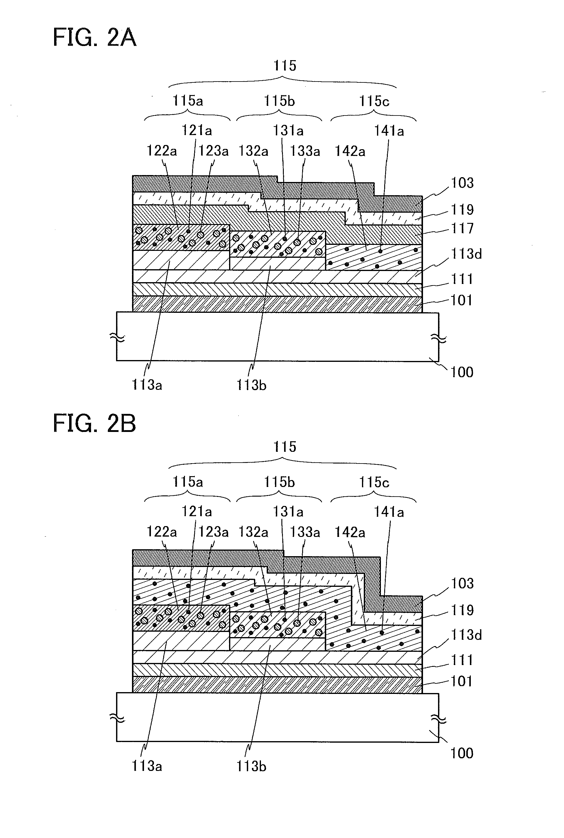
[0103]In this embodiment, modification examples of the light-emitting elements of one embodiment of the present invention in FIGS. 1A and 1B are described with reference to FIGS. 2A and 2B and FIGS. 3A and 3B. Note that portions similar to those in the above embodiments and portions having functions similar to those in the above embodiments are given the same reference numerals, and detailed description thereof is omitted.

[0104]A light-emitting element illustrated in FIG. 2A includes the light-emitting layer 115 between a pair of electrodes (the anode 101 and the cathode 103). The light-emitting layer 115 includes the first light-emitting layer 115a including the first phosphorescent material 121a and the first electron-transport material 122a; the second light-emitting layer 115b including the second phosphorescent material 131a and the second electron-transport material 132a; and the third light-emitting layer 115c including the fluorescent material 141a and the third electron-tra...

embodiment 3

[0136]In this embodiment, a light-emitting device manufactured using the light-emitting element of one embodiment of the present invention is described with reference to FIGS. 4A and 4B.

[0137]FIGS. 4A and 4B are cross-sectional views of light-emitting devices 250 and 260 in which first to third light-emitting layers are provided between an anode and a cathode.

[0138]First, the light-emitting device 250 illustrated in FIG. 4A is described below.

[0139]The light-emitting device 250 is what is called a bottom-emission light-emitting device in which light can be extracted from a substrate 200 side (a side indicated by arrows in FIG. 4A).

[0140]The light-emitting device 250 includes anodes 201a, 201b, and 201c that have shapes of separated islands, over the substrate 200. The material of the substrate 100 described in Embodiment 1 can be used for the substrate 200. The material of the anode 101 described in Embodiment 1 can be used for the anodes 201a, 201b, and 201c. The anodes 201a, 201b,...


PUM


Abstract

A light-emitting element which includes a plurality of light-emitting layers between a pair of electrodes and has low driving voltage and high emission efficiency is provided. A light-emitting element including first to third light-emitting layers between a cathode and an anode is provided. The first light-emitting layer includes a first phosphorescent material and a first electron-transport material; the second light-emitting layer includes a second phosphorescent material and a second electron-transport material; the third light-emitting layer includes a fluorescent material and a third electron-transport material; the first to third light-emitting elements are provided in contact with an electron-transport layer positioned on a cathode side; and a triplet excitation energy level of a material included in the electron-transport layer is lower than triplet excitation energy levels of the first electron-transport material and the second electron-transport material.

Description

BACKGROUND OF THE INVENTION[0001]1. Field of the Invention[0002]One embodiment of the present invention relates to a light-emitting element in which a light-emitting layer capable of emitting light by application of an electric field is provided between a pair of electrodes, and also relates to a light-emitting device and a lighting device including such a light-emitting element.[0003]2. Description of the Related Art[0004]Light-emitting elements which include organic compounds as a light-emitting layer and are characterized by thinness, lightweight, fast response, and direct current driving with low voltage are expected to be applied to next-generation flat panel displays. In particular, a display device in which light-emitting elements are arranged in matrix is considered to have advantages in a wide viewing angle and excellent visibility over a conventional liquid crystal display device.[0005]It is said that a light-emitting element has the following light emission mechanism: whe...

Claims


Application Information

Patent Timeline
Patent Type & Authority Applications(United States)
IPC IPC(8): H01L51/00
CPCH01L51/0085H10K85/622H10K85/633H10K85/631H10K85/6576H10K85/342H10K85/6572H10K50/13H10K50/11H10K2101/10H10K50/16H10K2101/27H10K2101/90H10K2101/30
Inventor SUZUKI, TSUNENORIHASHIMOTO, NAOAKISAIJO, ERIKOSEO, SATOSHI
Owner SEMICON ENERGY LAB CO LTD
Why Eureka
Try Eureka