Optical device and method for manufacturing same

a technology of optical devices and optical crystallization, which is applied in the manufacture of semiconductor/solid-state devices, semiconductor devices, electrical equipment, etc., can solve the problems of low price competitiveness of led, difficult to manufacture led on a large area, and difficult to employ light-emitting semiconductors as large-area display devices or light sources for illuminators. achieve the effect of high crystallinity

Active Publication Date: 2014-10-02
SEOUL NAT UNIV R&DB FOUND
View PDF4 Cites 6 Cited by
  • Summary
  • Abstract
  • Description
  • Claims
  • Application Information

AI Technical Summary

Benefits of technology

[0016]The present invention can provide an optical device and a method of manufacturing the same in which after a graphite layer is formed on a transparent amorphous substrate, a semiconductor unit is formed, and problems caused by the formation of a semiconductor unit on a conventional amorphous substrate can be resolved, yielding a semiconductor unit having a high crystallinity. Also, by controlling the thicknesses of the current injection layer and the graphite layer, the advantages of the transparent amorphous substrate can be maximized so that a direction of light emitted by or absorbed in the optical device can be controlled.

Problems solved by technology

However, it is difficult to employ a light-emitting semiconductor as a large-area display device or as a light source for an illuminator.
In particular, it is difficult to manufacture an LED on a large area, and the LED has low price competitiveness.
Since the LED uses a single crystalline substrate, fabrication costs are high and limitations with the sizes of products are problematic.
However, it is difficult to manufacture a highly efficient LED using a nitride semiconductor material on an amorphous substrate.
Accordingly, an LED using a polycrystalline nitride thin layer is inferior in device characteristics and efficiency to an LED using a single crystalline nitride semiconductor material manufactured on a single crystalline sapphire substrate.

Method used


Image

  • Optical device and method for manufacturing same
  • Optical device and method for manufacturing same
  • Optical device and method for manufacturing same

Examples


Embodiment Construction

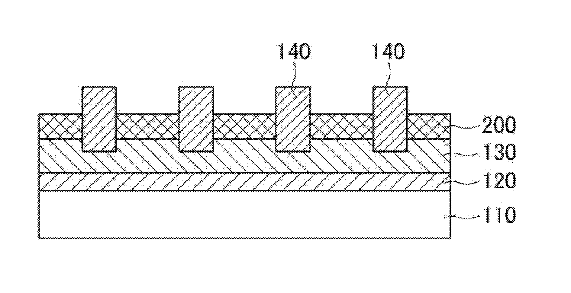
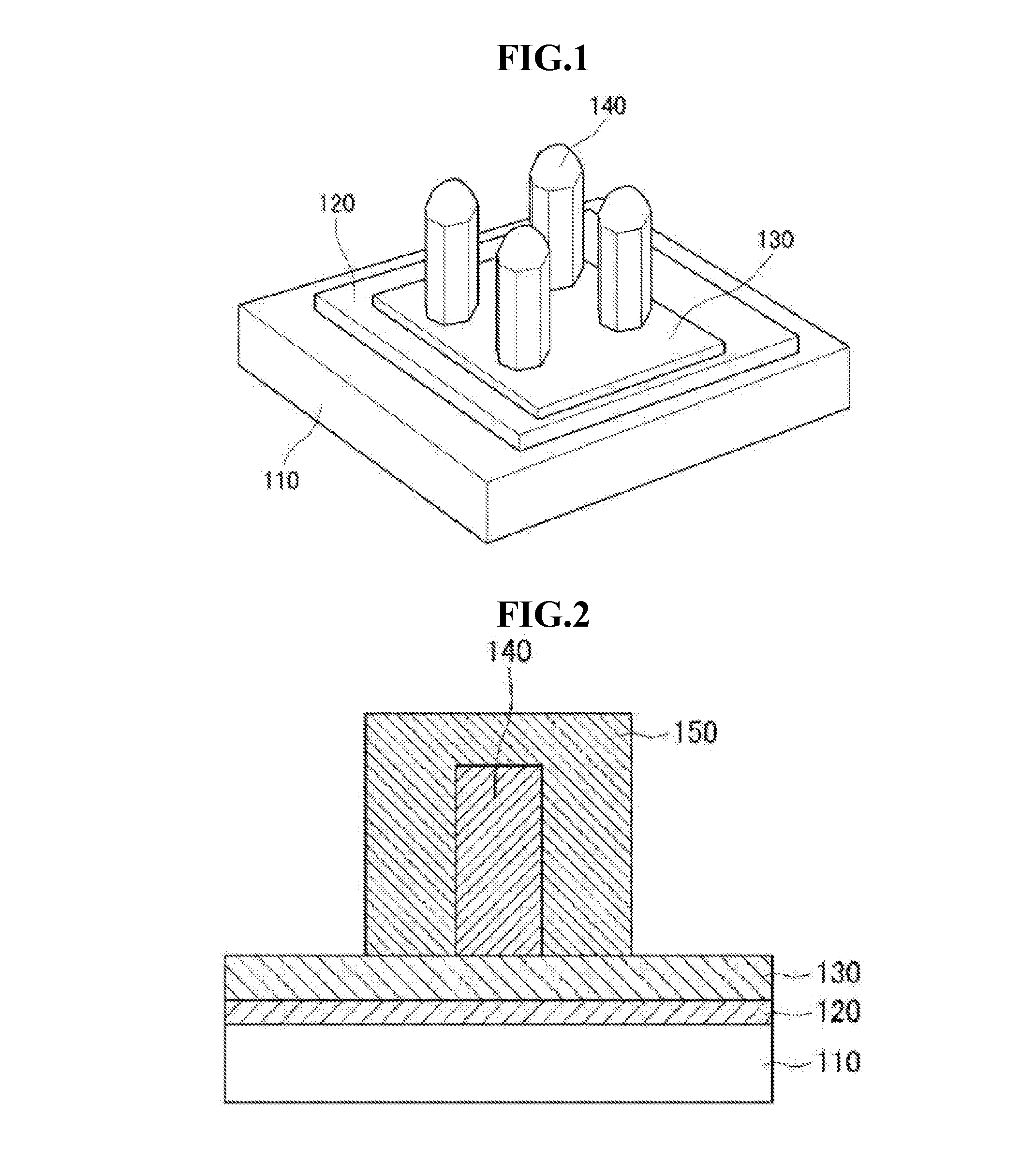
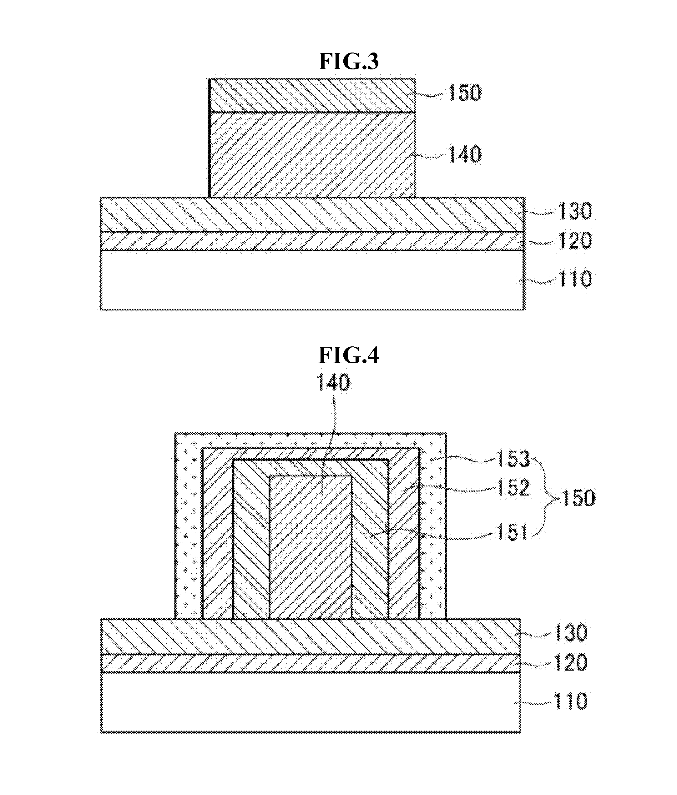
[0022]Hereinafter, exemplary embodiments of the present invention will be described in detail. However, the present invention is not limited to the exemplary embodiments disclosed below, but can be implemented in various types. Therefore, the present exemplary embodiments are provided for complete disclosure of the present invention and to fully describe the scope of the present invention to those of ordinarily skill in the art. Descriptions of irrelevant components are omitted from the drawings so as to clearly describe the exemplary embodiments of the present invention. Like elements are denoted by like reference numerals in the drawings.

[0023]Throughout this specification, it will be understood that when an element is referred to as being “connected” to another element, it can be “directly connected” to the other element or “electrically connected” to the other element with other elements therebetween. It will be further understood that when an element is referred to as “comprise...


PUM

PropertyMeasurementUnit
temperaturesaaaaaaaaaa
angleaaaaaaaaaa
conductiveaaaaaaaaaa

Abstract

Provided are an optical device and a method for manufacturing same. The optical device according to the present invention including: a transparent amorphous substrate; a current injection layer formed on the substrate; a graphite layer formed on the current injection layer; and a semiconductor unit formed on the graphite layer, wherein the semiconductor unit is formed after forming the graphite layer on the amorphous substrate, thereby overcoming the problems of conventional methods that involve forming a semiconductor unit on an amorphous substrate, and the semiconductor unit of the present invention has superior crystallinity.

Description

CROSS REFERENCE TO RELATED APPLICATIONS AND CLAIM OF PRIORITY[0001]This patent application is a National Phase application under 35 U.S.C. §371 of International Application No. PCT / KR2012 / 006484, filed Aug. 14, 2012, which claims priority to Korean Patent Application No. 10-2011-0081270 filed Aug. 16, 2011, entire contents of which are incorporated herein by reference.BACKGROUND[0002]1. Field of the Invention[0003]The present invention relates to an optical device and a method for manufacturing the same.[0004]2. Description of the Related Art[0005]Since a light-emitting diode (LED) is highly efficient and has a long lifespan, the LED drastically reduces energy consumption and has attracted much attention as an environmentally friendly optical device.[0006]Recently, advanced display devices and illuminators have been developed using light-emitting diodes (LEDs), and in addition, LEDs in portable phone keypads / flashes and automobile headlights / pilot lights have been manufactured.[0007...

Claims


Application Information

Patent Timeline
Patent Type & Authority Applications(United States)
IPC IPC(8): H01L33/24H01L33/32H01L33/00
CPCH01L33/24H01L33/32H01L33/007H01L33/08H01L33/02
Inventor YI, GYU-CHULCHUNG, KUNOOK
Owner SEOUL NAT UNIV R&DB FOUND
Why Eureka
Try Eureka