Conductive sheet and touch panel

a technology of conductive sheets and touch panels, applied in the direction of dielectric characteristics, circuit optical details, instruments, etc., can solve the problems of unfavorable visibility and lower detection performance of finger contact in some cases, and achieve the effect of suppressing visibility and high detection accuracy

Active Publication Date: 2014-10-09
FUJIFILM CORP
View PDF3 Cites 70 Cited by
  • Summary
  • Abstract
  • Description
  • Claims
  • Application Information

AI Technical Summary

Benefits of technology

[0048]The conductive sheets according to the above-mentioned aspects and the capacitive touch panel can suppress a decrease in visibility.
[0049]According to the presen

Problems solved by technology

However, in a touch panel of U.S. Patent Application Publication No. 2004/0229028, in the case where an upper electrode is made of a uniform conductive region and does not have a nonconductive region, even if a finger or the like comes into contact with the touch panel, lines of discharged electri

Method used


Image

  • Conductive sheet and touch panel
  • Conductive sheet and touch panel
  • Conductive sheet and touch panel

Examples


first embodiment

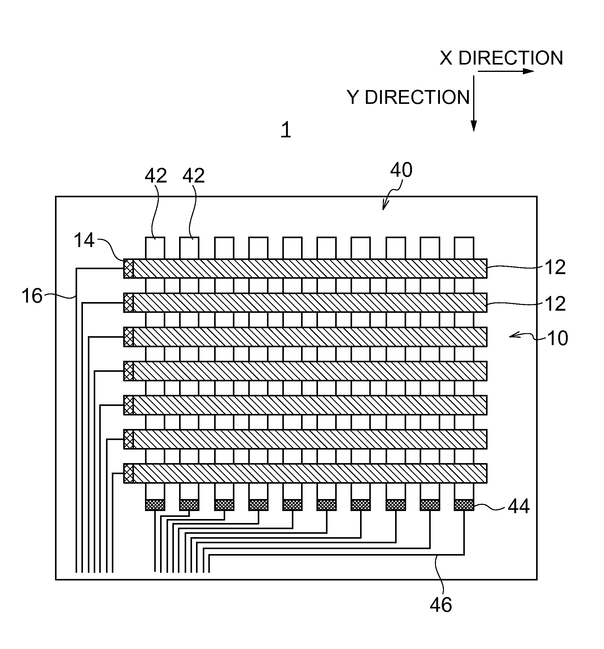
[0099]FIG. 5 illustrates a conductive sheet 1 including a first electrode pattern 10 according to a first embodiment. In FIG. 5, the first electrode pattern 10 includes two types of first conductive patterns 12 formed by a plurality of grids 26 made of metal thin wires. The plurality of grids 26 have substantially uniform shapes. Here, the substantially uniform means not only that the shapes are completely coincident with each other but also that the shapes and sizes of the grids 26 are seemingly the same as each other.

[0100]Each first conductive pattern 12 has one end electrically connected to a first electrode terminal 14. Each first electrode terminal 14 is electrically connected to one end of each first wire 16. Each first wire 16 has another end electrically connected to a terminal 20. Each first conductive pattern 12 is electrically separated by a first nonconductive pattern 28.

[0101]Note that, in the case of the use of the conductive sheet 1 as a transparent conductive film p...

second embodiment

[0132]FIG. 12 illustrates a conductive sheet 1 including a first electrode pattern 10 according to another embodiment. Configurations similar to those in FIG. 5 are designated by the same reference numerals or reference characters, and description thereof may be omitted. In FIG. 12, the first electrode pattern 10 includes two types of first conductive patterns 12 formed by a plurality of grids 26 made of metal thin wires. The plurality of grids 26 have substantially uniform shapes. Here, the substantially uniform means not only that the shapes are completely coincident with each other but also that the shapes and sizes of the grids 26 are seemingly the same as each other.

[0133]Each first conductive pattern 12 has one end electrically connected to a first electrode terminal 14. Each first electrode terminal 14 is electrically connected to one end of each first wire 16. Each first wire 16 has another end electrically connected to a terminal 20. Each first conductive pattern 12 is elec...

examples

[0372]Hereinafter, the present invention is further specifically described by way of examples of the present invention. Note that materials, usage amounts, percentages, processing contents, processing procedures, and the like described in the following examples can be changed as appropriate within a range not departing from the gist of the present invention. Accordingly, the scope of the present invention should not be limitatively interpreted by way of the following specific examples.

[0373]

[0374](Silver Halide Photosensitive Material)

[0375]Prepared was an emulsion containing 10.0 g of gelatin for 150 g of Ag in an aqueous medium and containing silver iodobromochloride grains (I=0.2 mol %, Br=40 mol %) having a sphere-equivalent diameter of 0.1 μm on average.

[0376]Moreover, K3Rh2Br9 and K2IrCl6 were added to the emulsion at a concentration of 1×10⁻⁷ (mole / mole silver), and the silver bromide grains were doped with Rh ions and Ir ions. Na2PdCl4 was added to the emulsion, and was furt...


PUM


Abstract

A conductive sheet includes: a substrate having a first main surface and a second main surface; and a first electrode pattern placed on the first main surface of the substrate. The first electrode pattern is made of metal thin wires, and includes a plurality of first conductive patterns that extend in a first direction. Each first conductive pattern includes, at least, inside thereof, a sub-nonconduction pattern that is electrically separated from the first conductive pattern. An area A of each first conductive pattern and an area B of each sub-nonconduction patterns satisfy a relation of 5%<B/(A+B)<97%. Accordingly, a conductive sheet and a touch panel having a high detection accuracy can be provided.

Description

CROSS-REFERENCE TO RELATED APPLICATIONS[0001]This application is a Continuation of PCT International Application No. PCT / JP2012 / 083222 filed on Dec. 21, 2012, which claims priorities under 35 U.S.C §119(a) to Japanese Patent Application No. 2011-281928 filed Dec. 22, 2011, Japanese Patent Application No. 2012-113741 filed May 17, 2012, and Japanese Patent Application No. 2012-182678 filed Aug. 21, 2012. Each of the above application(s) is hereby expressly incorporated by reference, in its entirety, into the present application.BACKGROUND OF THE INVENTION[0002]1. Field of the Invention[0003]The present invention relates to a conductive sheet and a touch panel.[0004]2. Description of the Related Art[0005]In recent years, touch panels are frequently used as input devices for portable terminals and computers. Such a touch panel is placed on a surface of a display, and performs an input operation by detecting a position touched with a finger or the like. For example, a resistance film ty...

Claims


Application Information

Patent Timeline
IPC IPC(8): H05K1/02
CPCH05K1/0296G06F3/044G06F2203/04103G06F2203/04112H05K2201/09681G06F3/0445G06F3/0446H05K1/0274H05K1/0289H05K2201/0108H05K2201/09781
Inventor NAKAMURA, HIROSHIGEKURIKI, TADASHI
Owner FUJIFILM CORP
Why Eureka
Try Eureka