Transparent capacitive touch panel

a capacitive touch panel and transparent technology, applied in the field of touch panels, can solve the problems of unfavorable image shown on displays will be distorted, foggy or even glaring, and even light passing through the conductive layer, so as to improve the optical properties of touch panels

Inactive Publication Date: 2014-10-09
YOUNG FAST OPTOELECTRONICS
View PDF7 Cites 10 Cited by
  • Summary
  • Abstract
  • Description
  • Claims
  • Application Information

AI Technical Summary

Benefits of technology

[0006]An object of the invention is to provide a transparent capacitive touch panel, which possesses an even RI. This can improve optical properties of a touch panel.
[0007]Another object of the invention is to provide a transparent capacitive touch panel, which has a thicker insulative layer to increase insulation ability and to avoid deformation.
[0012]In a preferred embodiment, the insulative layer is composed of a plurality of insulative coatings. Such multiple coatings not only are easy to be processed, but also can increase thickness and insulation effect. The coatings may be made of two or more different materials. This can modify the overall refractive index of the insulative layer to match the conductive layer. Preferably, the coatings are three or an odd number more than three in number, and the odd layers are made of the same insulative material. This can balance the internal stress between coatings and avoid deformation. Additionally, each of the insulative layers is composed of a plurality of insulative coatings, and each coating is less than 100 nm in thickness. This can reduce internal stress to avoid deformation.
[0013]In an embodiment, the insulative layer is a transparent insulative bond, for example a polymeric optically clear adhesive (OCA) containing silicon dioxide (SiO2), aluminum oxide (Al2O3) or niobium pentoxide (Nb2O5). Such a insulative bond can firmly combine every layer and provide insulation between two adjacent layers. When the insulative bond is liquid and daubed on the conductive layers, the insulative bond can easily fill the gaps of the conductive layers to increase evenness of the RI of the conductive layers.

Problems solved by technology

This will cause uneven refraction of light passing through the conductive layer.
As a result, the image shown on a display will be distorted, foggy or even glaring.

Method used


Image

  • Transparent capacitive touch panel
  • Transparent capacitive touch panel
  • Transparent capacitive touch panel

Examples


Embodiment Construction

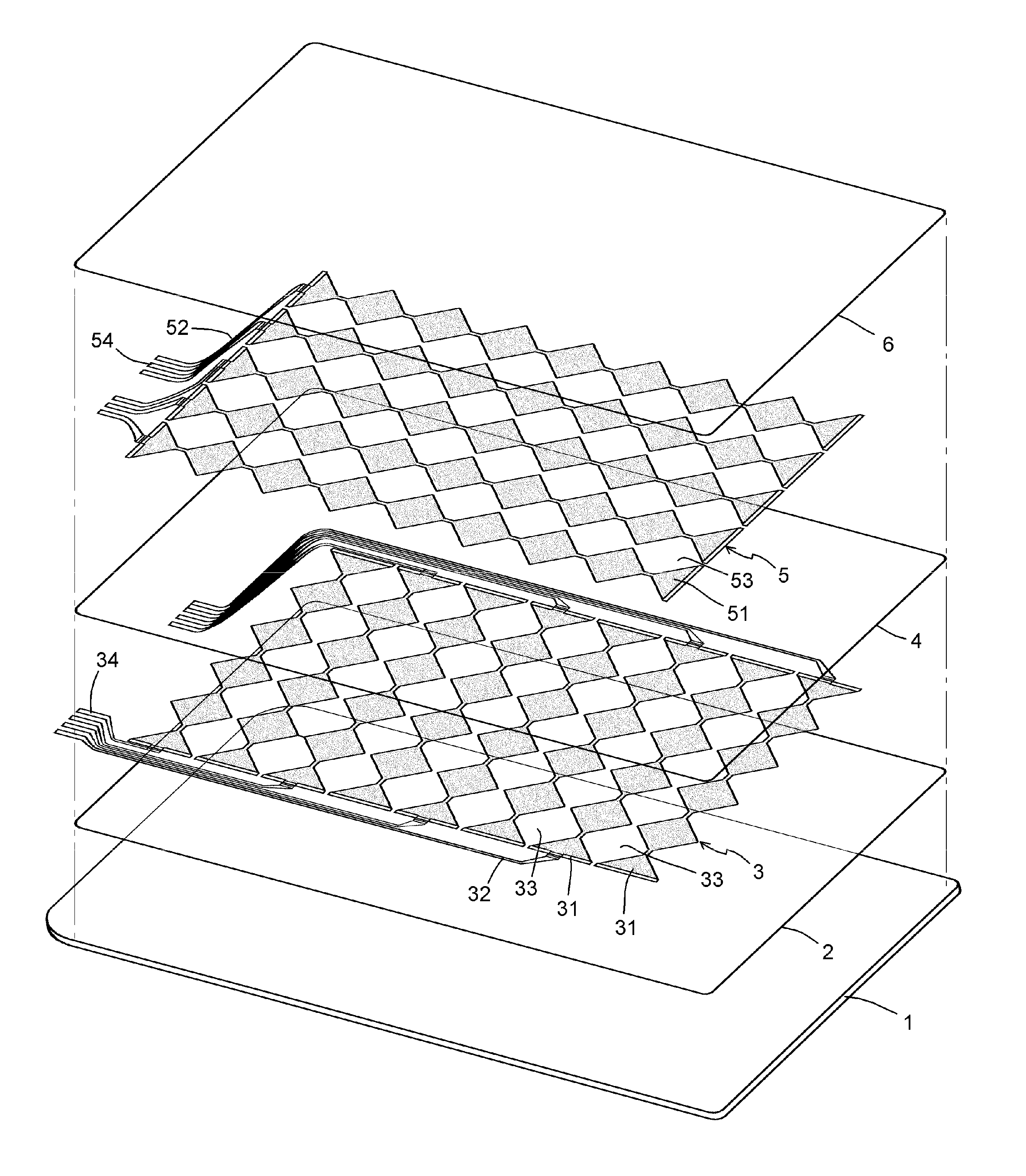
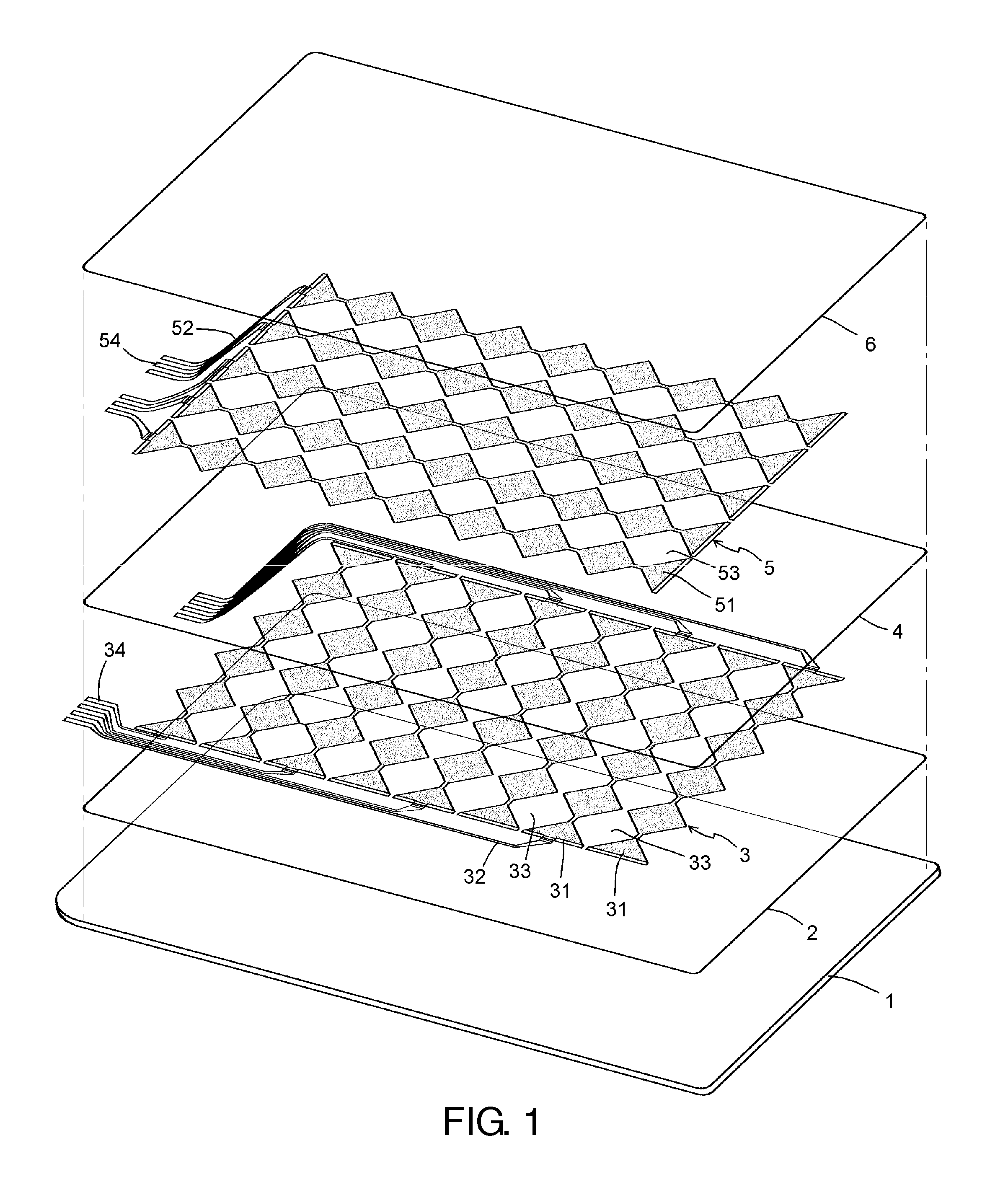
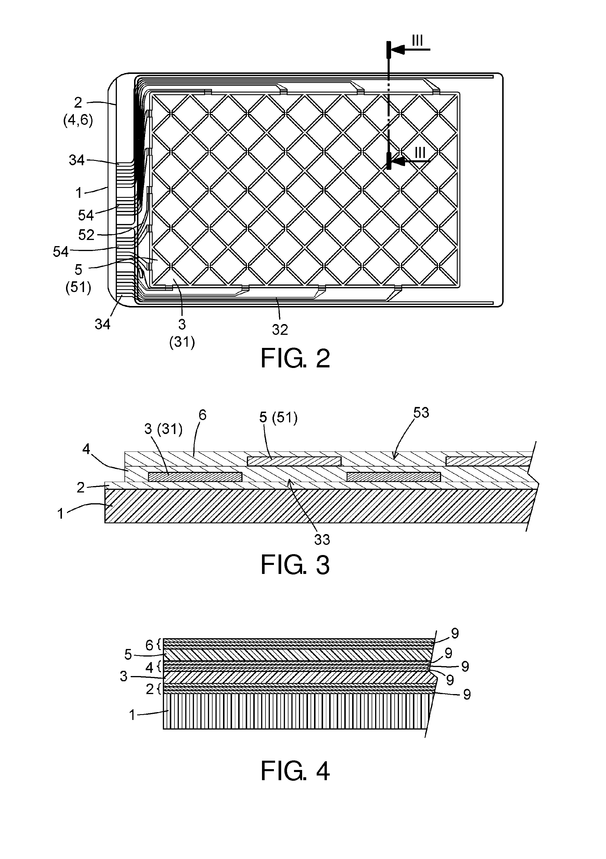
[0020]Please refer to FIGS. 1-3. The invention forms a fundamental insulative layer 2, an X-axis conductive layer 3, an intermediate insulative layer 4, a Y-axis transparent conductive layer 5, and a protective insulative layer 6 in sequence on a substrate 1.

[0021]The substrate 1 may use soda lime glass with a refractive index (RI) of about 1.5.

[0022]The X-axis and Y-axis conductive layers 3, 5 may use indium tin oxide (ITO). There are transparent X-axis capacitive sensor rows 31 at a constant interval along X-axis on the X-axis conductive layer 3. A gap 33 is remained between every two adjacent X-axis capacitive sensor rows 31. The gaps 33 divide the X-axis capacitive sensor rows 31 to be insulated. Ends of the X-axis capacitive sensor rows 31 are electrically separately connected with signal wires 32 with signal output ends 34. Similarly, there are transparent Y-axis capacitive sensor rows 51 at a constant interval along Y-axis on the Y-axis conductive layer 5. A gap 53 is remaine...


PUM


Abstract

The capacitive touch panel includes a transparent substrate, a first transparent conductive layer, a first transparent insulative layer, a second transparent conductive layer, and a second transparent insulative layer. Each transparent conductive layer has a plurality of capacitive sensor rows. Every adjacent two of the capacitive sensor rows are formed with a gap to be insulated. The transparent insulative layers have a refractive index equal to or greater than that of the transparent conductive layers and fill the gaps. Each of the insulative layers is composed of a plurality of insulative coatings, and each coating is less than 100 nm in thickness.

Description

BACKGROUND OF THE INVENTION[0001]1. Technical Field[0002]The invention relates to touch panels for LCDs, particularly to transparent capacitive touch panels.[0003]2. Related Art[0004]In a typical capacitive touch panel, the two capacitive sensor rows along X-axis and Y-axis are arranged on two different conductive layers, and the two conductive layers are insulatedly superposed on a substrate. On each conductive layer, there are a plurality of capacitive sensor rows along the same axis, and all other material except the conductive sensor rows is removed to form gaps. Thus, every two adjacent capacitive sensor rows are insulated by the gaps.[0005]To make a touch panel suitable for being installed before a display of an electronic device, usually the substrate is made of transparent glass and indium tin oxide (ITO) is used to be a conductive layer. As abovementioned, the pattern on the conductive layer includes an ITO material (i.e. capacitive sensor rows) and gaps. Because the ITO ma...

Claims


Application Information

Patent Timeline
Patent Type & Authority Applications(United States)
IPC IPC(8): G06F1/16G02B1/10
CPCG02B1/10G06F1/169G06F3/0445G06F3/0446
Inventor YANG, KAI-TI
Owner YOUNG FAST OPTOELECTRONICS
Why Eureka
Try Eureka