Multilayer ceramic capacitor and method of manufacturing the same

a ceramic capacitor and multi-layer technology, applied in the direction of fixed capacitors, stacked capacitors, fixed capacitor details, etc., can solve the problems of difficult carbon removal, limited overlapped area of internal electrodes, and high cost, and achieve excellent reliability

Active Publication Date: 2014-10-09
SAMSUNG ELECTRO MECHANICS CO LTD
View PDF6 Cites 46 Cited by
  • Summary
  • Abstract
  • Description
  • Claims
  • Application Information

AI Technical Summary

Benefits of technology

[0015]An aspect of the present invention provides a high-capacitance multilayer ceramic capacitor having excellent reliability, and a method of manufacturing the same.

Problems solved by technology

In the case of manufacturing a multilayer ceramic capacitor through the above-described manufacturing method, since it is difficult to significantly decrease a margin part region of the dielectric layer on which the internal electrode is not formed, there is a limitation in increasing the overlapped area of the internal electrodes.
In addition, since the margin part of an edge of the multilayer ceramic capacitor is formed to be thicker than margin parts in other regions, it is not easy to remove carbon therefrom at the time of calcining and sintering.
In order to solve the above-described problems, a method, in which the margin part region on which the internal electrode is not formed is formed in the previously manufactured ceramic multilayer body, has been considered, but the ceramic multilayer body may be vulnerable to impact due to pores generated in a boundary surface between a cover region of the ceramic multilayer body and the margin part.
A ceramic multilayer body of which a porosity of a cover region is controlled is disclosed in the following Related Art Document, but the above-mentioned problem may not be solved.

Method used


Image

  • Multilayer ceramic capacitor and method of manufacturing the same
  • Multilayer ceramic capacitor and method of manufacturing the same
  • Multilayer ceramic capacitor and method of manufacturing the same

Examples


Embodiment Construction

[0035]Hereinafter, embodiments of the present invention will be described in detail with reference to the accompanying drawings. The invention may, however, be embodied in many different forms and should not be construed as being limited to the embodiments set forth herein. Rather, these embodiments are provided so that this disclosure will be thorough and complete, and will fully convey the scope of the invention to those skilled in the art.

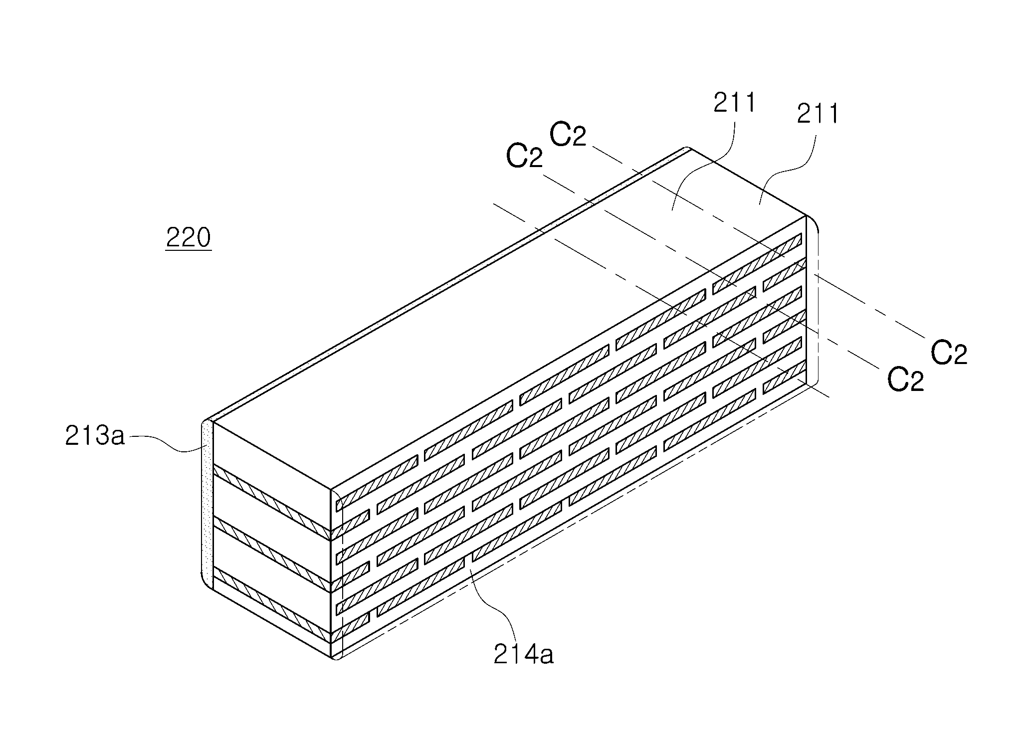
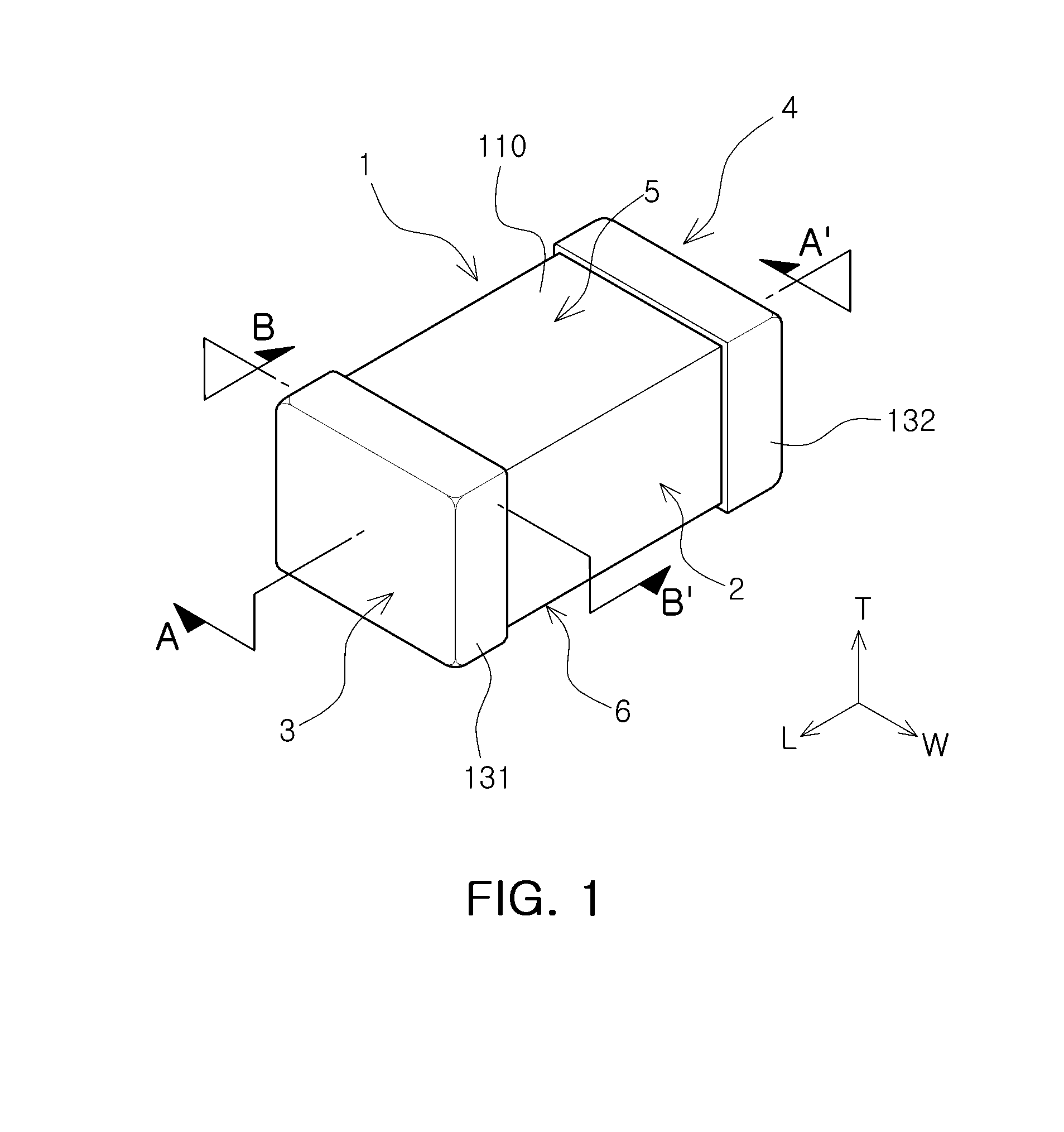
[0036]FIG. 1 is a schematic perspective view showing a multilayer ceramic capacitor according to an embodiment of the present invention.

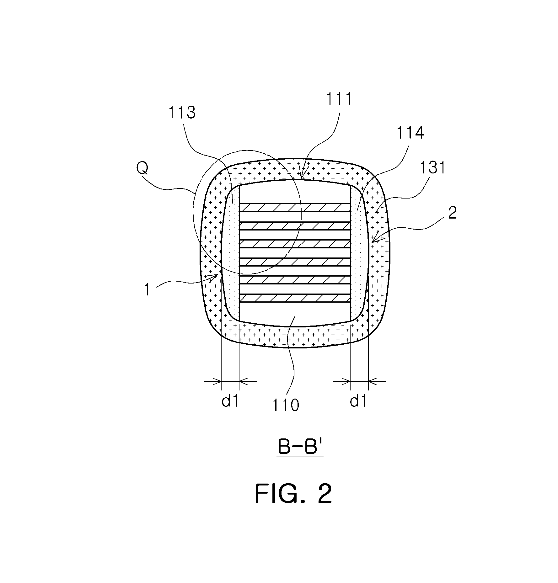
[0037]FIG. 2 is a cross-sectional view taken along line B-B′ of FIG. 1.

[0038]FIG. 3 is an enlarged view of part Q of FIG. 2.

[0039]FIG. 4 is a cross-sectional view taken along line A-A′ of FIG. 1, and FIG. 5 is an upper plan view showing a dielectric layer configuring the multilayer ceramic capacitor shown in FIG. 1.

[0040]Referring to FIGS. 1 through 5, the multilayer ceramic capacitor according to the embodiment...


PUM

PropertyMeasurementUnit
thicknessaaaaaaaaaa
distance d1aaaaaaaaaa
lengthaaaaaaaaaa

Abstract

There is provided a multilayer ceramic capacitor including a ceramic body having first and second side surfaces and third and fourth end surfaces, a plurality of internal electrodes and having one ends exposed to the third or fourth end surface, and first and second side margin parts formed so that an average thickness from the first and second side surfaces to edges of the internal electrodes is 18 μm or less, wherein when the first or second side margin part is divided into two regions by a virtual line obtained by connecting mid points of distances between the edges of the internal electrodes and points at which lines extended from the internal electrodes contact the first or second side surface, when a region adjacent to the internal electrodes is defined as S1 and a porosity of S1 is defined as P1, P1 is in a range of 1 to 20 (1≦P1≦20).

Description

CROSS-REFERENCE TO RELATED APPLICATION[0001]This application claims the priority of Korean Patent Application No. 10-2013-0038320 filed on Apr. 8, 2013, in the Korean Intellectual Property Office, the disclosure of which is incorporated herein by reference.BACKGROUND OF THE INVENTION[0002]1. Field of the Invention[0003]The present invention relates to a multilayer ceramic capacitor and a method of manufacturing the same, and more particularly, to a high capacitance multilayer ceramic capacitor having excellent reliability, and a method of manufacturing the same.[0004]2. Description of the Related Art[0005]Generally, electronic components using a ceramic material, such as a capacitor, an inductor, a piezoelectric element, a varistor, a thermistor, or the like, include a ceramic body formed of a ceramic material, internal electrodes formed in the ceramic body, and external electrodes mounted on external surfaces of the ceramic body so as to be connected to the internal electrodes.[000...

Claims


Application Information

Patent Timeline
Patent Type & Authority Applications(United States)
IPC IPC(8): H01G4/01H01G4/30
CPCH01G4/30H01G4/01H01G4/012H01G4/12H01G4/232
Inventor KIM, HYUNG JOON
Owner SAMSUNG ELECTRO MECHANICS CO LTD
Why Eureka
Try Eureka