Liquid crystal display device and drive method for same

a technology of liquid crystal display and drive method, which is applied in the direction of electric digital data processing, instruments, computing, etc., can solve the problems of deterioration in display quality, inability to transmit video signals indicating pixel values for a plurality of lines, and the above-mentioned method cannot be adopted with regard to the discharge of electric charges, etc., and achieves the effect of simple configuration

Inactive Publication Date: 2014-10-16
SHARP KK
View PDF6 Cites 28 Cited by
  • Summary
  • Abstract
  • Description
  • Claims
  • Application Information

AI Technical Summary

Benefits of technology

[0093]According to a first aspect of the present invention, when the supply of the power supply is shut off in the liquid crystal display device, two processings (first discharge processing and second discharge processing) for discharging the electric charges in the display panel are sequentially performed. In the first discharge processing, the potential of the clock signal and the reference potential are set at the first scanning signal line selection potential. Thus, the potential of the clock signal turned to the high level is given to the output node through the output control switching element, and accordingly, each of the scanning signal lines is turned to the selected state. At this time, by setting the video signal potential at the ground potential, the electric charges in the respective pixel formation portions are discharged. Moreover, the first scanning signal line selection potential is lowered to the ground potential before the second discharge processing is started. Therefore, in the event of the first discharge processing, the potential of the clock signal and the reference potential are gradually lowered, and the electric charges on the scanning signal lines are also discharged. In the second discharge processing, the potential of the clear signal is set at the second scanning signal line selection potential. At the point of time when the second discharge processing is started, the second scanning signal line selection potential is maintained at the potential level at which the switching elements included in each of the bistable circuits are turned to the ON state, and accordingly, the electric charges on the floating nodes (first node and second node) in each of the bistable circuits are discharged by the second discharge processing. In such a way as described above, the residual electric charges in the display panel are rapidly removed when the power supply is turned off, and an occurrence of display defect/malfunction that may

Problems solved by technology

Video signals, each of which indicates the pixel value, are transmitted by the source bus lines; however, each of the source bus lines cannot transmit video signals indicating pixel values for a plurality of rows at a time (simultaneously).
Moreover, when the power supply of the device is turned on in a state where the residual electric charges are accumulat

Method used


Image

  • Liquid crystal display device and drive method for same
  • Liquid crystal display device and drive method for same
  • Liquid crystal display device and drive method for same

Examples


Embodiment Construction

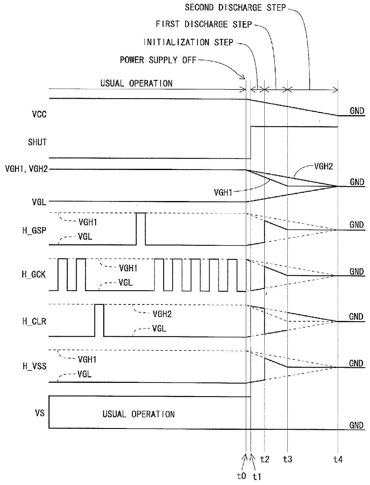
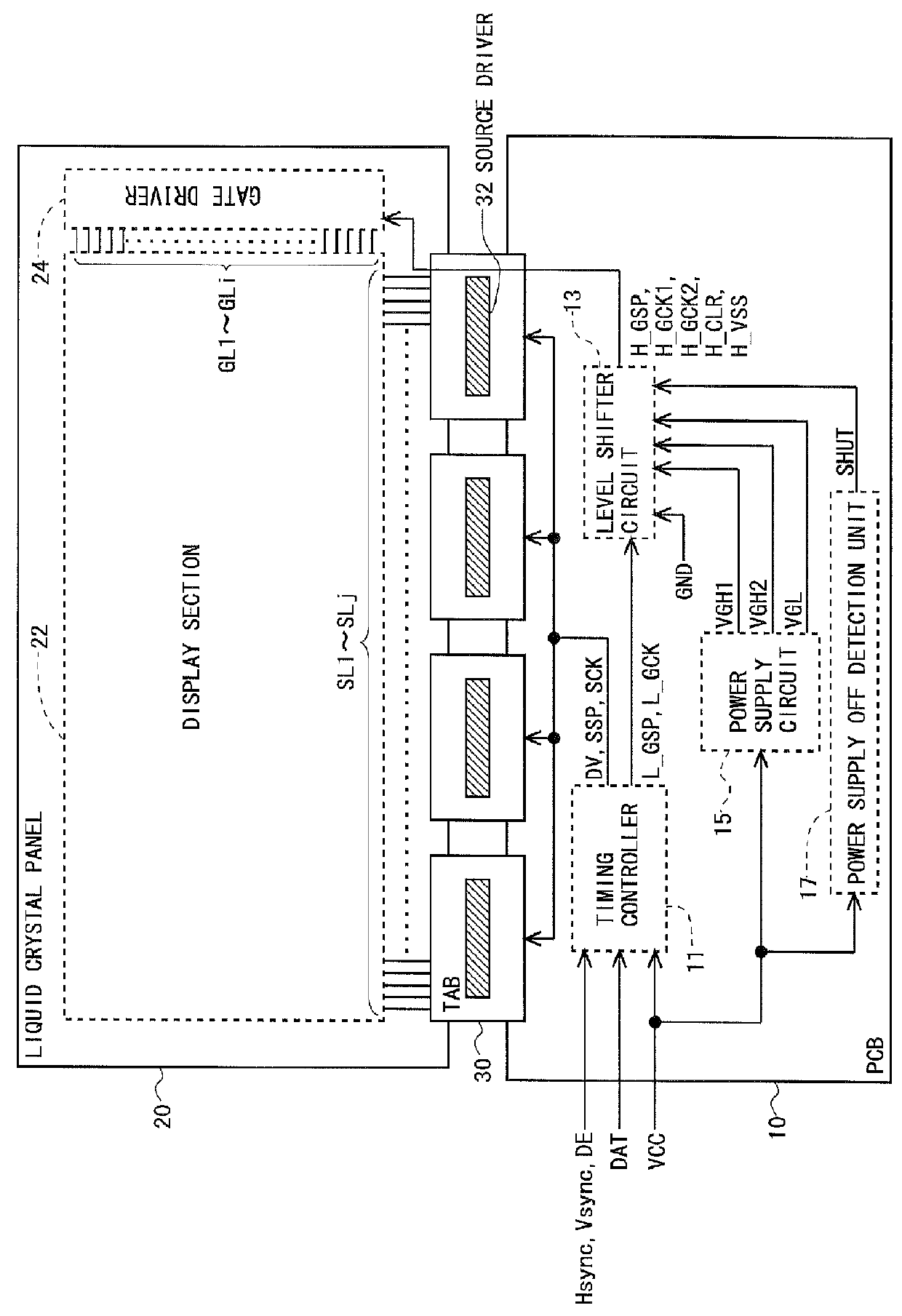
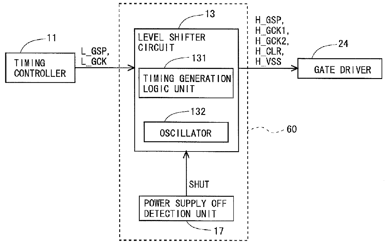
[0127]A description is made below of an embodiment of the present invention with reference to the accompanying drawings. Note that, in the following description, a gate terminal (gate electrode) of each of thin film transistors corresponds to a first electrode, a drain terminal (drain electrode) thereof corresponds to a second electrode, and a source terminal (source electrode) thereof corresponds to a third electrode. Moreover, the description is made on the assumption that all of thin film transistors provided in bistable circuits are of the n-channel type.

[0128]

[0129]FIG. 2 is a block diagram showing an entire configuration of an active matrix-type liquid crystal display device according to an embodiment of the present invention. As shown in FIG. 2, this liquid crystal display device is constituted by: a liquid crystal panel (display panel) 20; a PCB (printed circuit board) 10; and a TAB (Tape Automated Bonding) 30 connected to the liquid crystal panel 20 and the PCB 10. Note tha...


PUM


Abstract

Provided are: a liquid crystal display device capable of rapidly removing residual electric charges in a panel when a power supply is turned off, and in particular, suitable for a case where IGZO-GDM is adopted; and a driving method of the liquid crystal display device.
In the liquid crystal display device, when an OFF state of the power supply is detected, a power supply OFF sequence including an initialization step, a first discharge step and a second discharge step is executed. In the initialization step, only a clear signal (H_CLR) among GDM signals is set at a high level, and a state of each of bistable circuits which constitute a shift register is initialized. In the first discharge step, only the clear signal (H_CLR) among the GDM signals is set at a low level, all of gate bus lines are turned to a selected state, and electric charges in pixel formation portions are discharged. In the second discharge step, the clear signal (H_CLR) is set at the high level, and electric charges on floating nodes in each of the bistable circuits are discharged.

Description

TECHNICAL FIELD[0001]The present invention relates to a liquid crystal display device and a driving method thereof, and particularly, relates to a liquid crystal display device suitable for a case of adopting a monolithic gate driver having a thin film transistor that uses an oxide semiconductor (IGZO) for a semiconductor layer, and to a driving method thereof.BACKGROUND ART[0002]In general, an active matrix-type liquid crystal display device includes a liquid crystal panel made of two substrates which sandwich a liquid crystal layer therebetween. On one substrate of the two substrates, a plurality of gate bus lines (scanning signal lines) and a plurality of source bus lines (video signal lines) are arranged in a grid pattern, and a plurality of pixel formation portions are arranged in a matrix so as to correspond to the respective intersections of the plurality of gate bus lines and the plurality of source bus lines. Each of the pixel formation portions includes: a thin film transi...

Claims


Application Information

Patent Timeline
IPC IPC(8): G09G3/36
CPCG09G3/3648G09G3/3677G09G2310/0286G09G2330/02G09G2330/027G09G3/3696
Inventor IWAMOTO, AKIHISAMORII, HIDEKIMIZUNAGA, TAKAYUKINAKAMINAMI, KAZUYAHORIUCHI, SATOSHI
Owner SHARP KK
Why Eureka
Try Eureka