Grapho-epitaxy dsa process with dimension control of template pattern

a grapho-epitaxy and template pattern technology, applied in the field of semiconductor processing, can solve the problems of high defect level, large resist feature size, and inability to form high-resolution mandrels

Inactive Publication Date: 2014-10-23
ELPIS TECH INC
View PDF3 Cites 28 Cited by
  • Summary
  • Abstract
  • Description
  • Claims
  • Application Information

AI Technical Summary

Problems solved by technology

However, present techniques yield large inaccurate resist features, which cannot form high resolution mandrels.
Further, metal lift-off processes from resist features require metal deposition onto a neutral material layer leading to high defect levels and high line edge roughness (LER).
Employing e-beam resists to form resist patterns on top of the neutral material layer is not a manufacturable lithographic technique useful for device production.
With these techniques or potential techniques, the height and profile of the resist tends to be poor at presently achievable and useful line widths, and these techniques may result in damage to the neutral material layer needed for the formation of DSA films and other structures.

Method used


Image

  • Grapho-epitaxy dsa process with dimension control of template pattern
  • Grapho-epitaxy dsa process with dimension control of template pattern
  • Grapho-epitaxy dsa process with dimension control of template pattern

Examples


Embodiment Construction

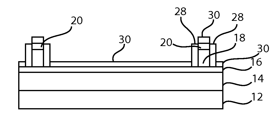
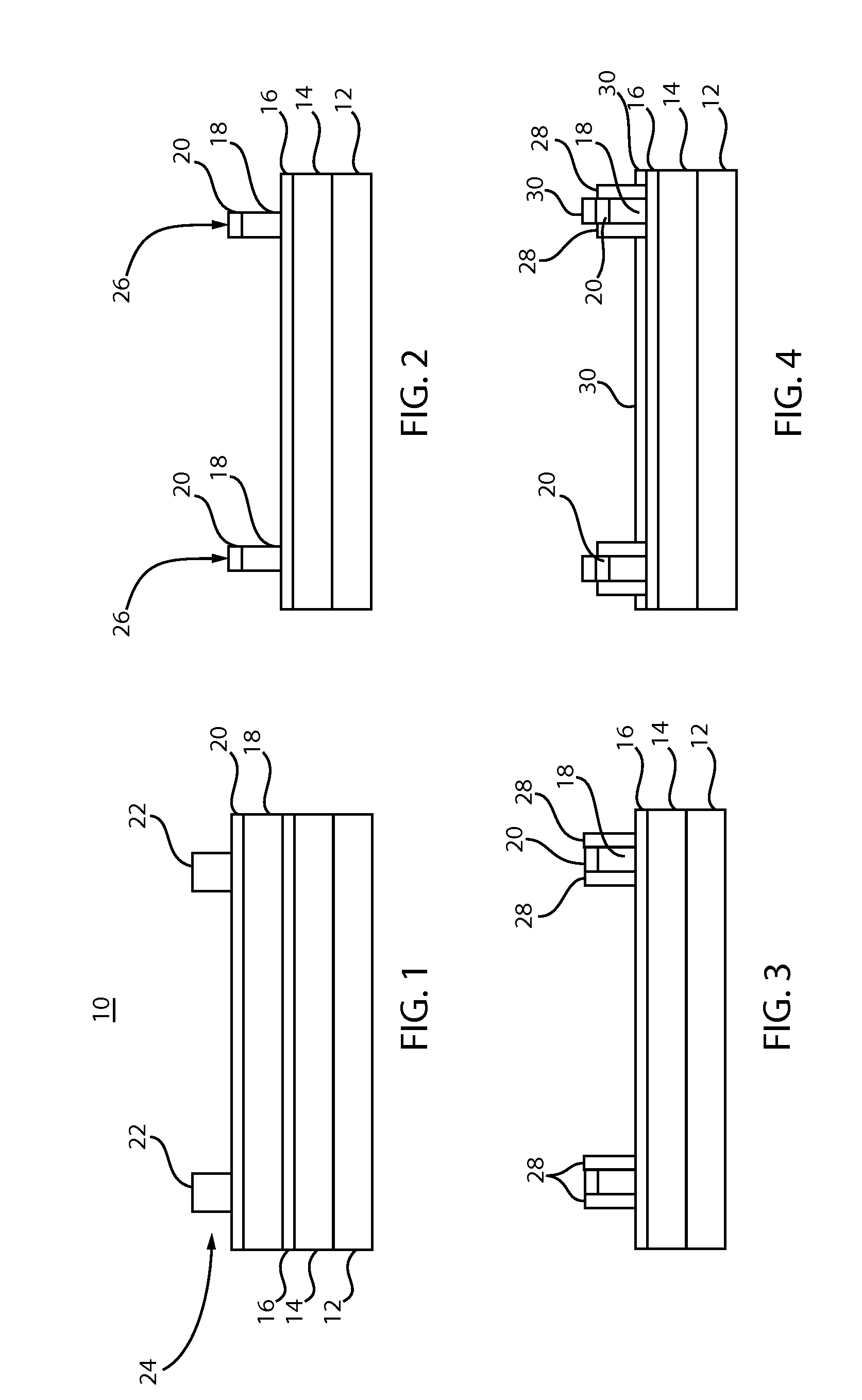
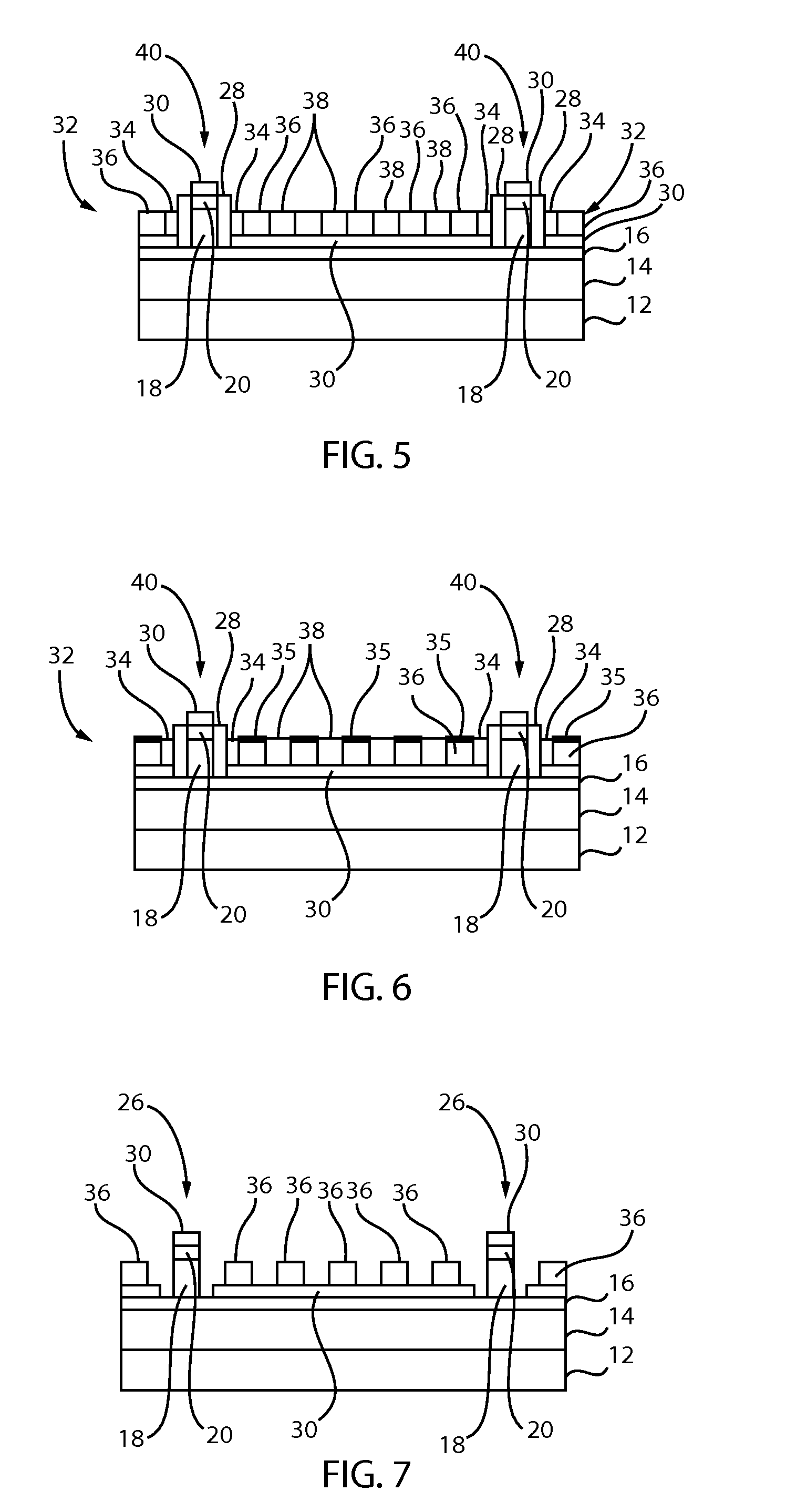
[0020]The present principles provide methods for forming templates with improved dimensional control. The templates may be provided for directed self-assembly (DSA) applications. In particularly useful embodiments, a dielectric stack is etched to form template lines. A substantially unreactive spacer is formed on sides of the template lines, which is employed to provide critical dimension control of the template line. DSA material is introduced between the spacers of the template lines and processed. A reactive ion etch (RIE) process may be employed to remove the spacers to provide an image reversed etch pattern for further etching, e.g., of a substrate or underlying layers.

[0021]In accordance with the present principles, an optical planarization layer (OPL) / silicon antireflection coating (ARC) stack may be patterned and combined with unreactive spacers (e.g., formed from a hydrophobic material with minimal hydroxyl groups) along sides of patterned stack. The patterned stack with sp...


PUM

PropertyMeasurementUnit
widthaaaaaaaaaa
widthaaaaaaaaaa
feature sizesaaaaaaaaaa

Abstract

A method for defining a template for directed self-assembly (DSA) materials includes patterning a resist on a stack including an ARC and a mask formed over a hydrophilic layer. A pattern is formed by etching the ARC and the mask to form template lines which are trimmed to less than a minimum feature size (L). Hydrophobic spacers are formed on the template lines and include a fractional width of L. A neutral brush layer is grafted to the hydrophilic layer. A DSA material is deposited between the spacers and annealed to form material domains in a form of alternating lines of a first and a second material wherein the first material in contact with the spacers includes a width less than a width of the lines. A metal is added to the domains forming an etch resistant second material. The first material and the spacers are removed to form a DSA template pattern.

Description

BACKGROUND[0001]1. Technical Field[0002]The present invention relates to semiconductor processing, and more particularly to methods for achieving high resolution resist structures for template formation for directed self-assembly (DSA) processing.[0003]2. Description of the Related Art[0004]Directed self-assembly (DSA) has emerged as a useful tool in semiconductor processing. DSA includes providing two materials and polymerizing them to concurrently form the materials into separate polymer regions. By providing physical guides, mandrels or templates, the polymers can be formed into useful structures, e.g., parallel lines and the like. DSA may be employed, e.g., to form interconnect lines, spacers and / or contacts.[0005]DSA typically requires high-resolution templates to ensure proper formation of the DSA structures. However, present techniques yield large inaccurate resist features, which cannot form high resolution mandrels. Further, metal lift-off processes from resist features req...

Claims


Application Information

Patent Timeline
Patent Type & Authority Applications(United States)
IPC IPC(8): H01L21/308
CPCH01L21/3081H01L21/0337G03F7/0002H01L21/3065H01L21/3086
Inventor ABDALLAH, JASSEM A.COLBURN, MATTHEW E.HOLMES, STEVEN J.LIU, CHI-CHUN
Owner ELPIS TECH INC
Why Eureka
Try Eureka