Inspection apparatus

Active Publication Date: 2014-10-30
NUFLARE TECH INC
View PDF3 Cites 2 Cited by
  • Summary
  • Abstract
  • Description
  • Claims
  • Application Information

AI Technical Summary

Benefits of technology

[0003]It is necessary to improve a production yield of the expensive LSI in a production process. In the semiconductor element, during a production process, an original graphic pattern (that is, a mask or a reticle, hereinafter collectively referred to as a mask) in which a circuit pattern is formed is exposed and transferred onto a wafer by a reduction projection exposure apparatus called a stepper or a scanner. A shape defect of a mask pattern and fluctuations of various process conditions while the pattern is exposed and transferred, ca

Problems solved by technology

A shape defect of a mask pattern and fluctuations of various process conditions while the pattern is exposed and transferred, can be cited as a large factor that reduces a production yield of the semiconductor element.
As a result, the objective lens is necessarily expanded in magnification and the depth of focus therefore becomes shallow.
In such a case, in the highly-magnified inspection apparatus, an image forming position of the defect varies, and sensitivity to the defect detection becomes unstable.
However, there are various heat generating sources in the inspection apparatus, and these sources may influence the inspection apparatus to cause fluctuations in temperature.
Such generated heat causes the inside of the inspection apparatus to loca

Method used


Image

  • Inspection apparatus
  • Inspection apparatus
  • Inspection apparatus

Examples


Example

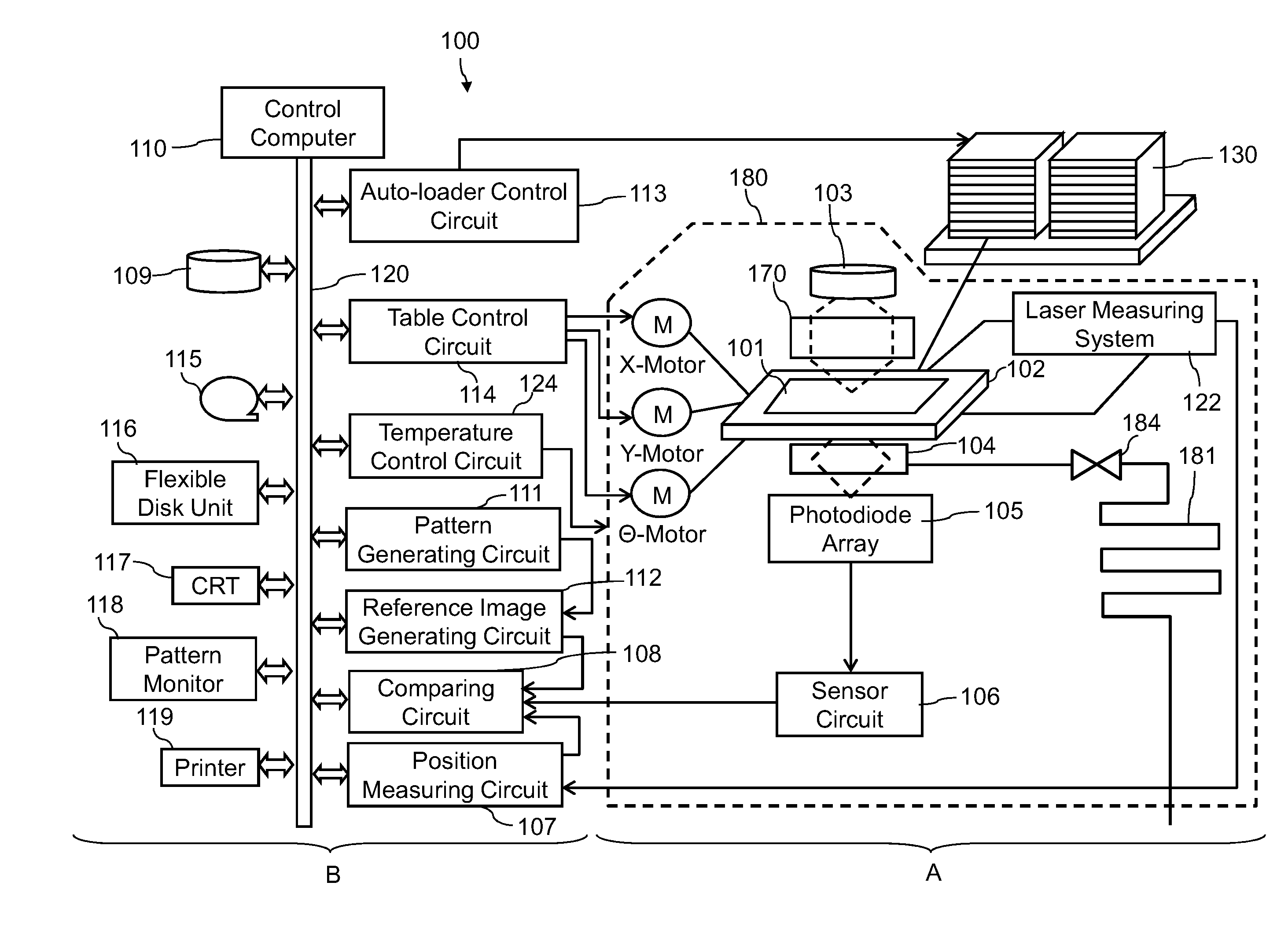
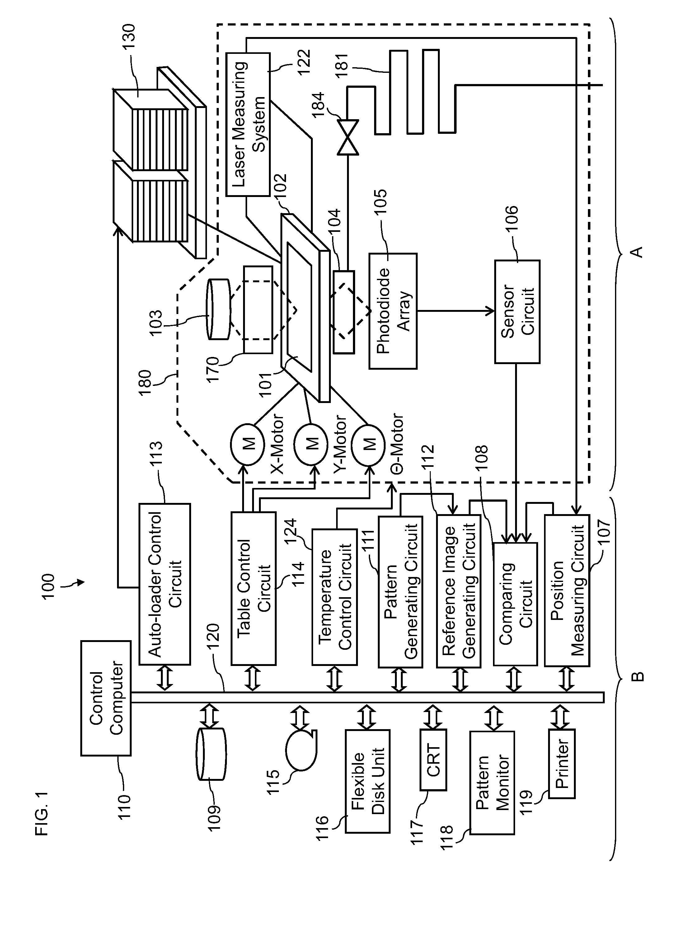
[0029]An inspection apparatus according to the first embodiment of the present invention will be described using the drawings.

[0030]FIG. 1 is a schematic configuration diagram of an inspection apparatus according to the first embodiment.

[0031]In FIG. 1, a configuration unit necessary in the present embodiment is illustrated. However, another well-known configuration unit necessary for an inspection may be used. As used herein, a “unit” or “circuit” can be configured by a program operating on a computer. Alternatively, the “unit” or “circuit” may be constructed by not only the program that is software, but also a combination of software and hardware, or software and firmware. In the case that the “unit” or “circuit” may be constructed by the program, the program can be recorded in a recording device such as a magnetic disk drive.

[0032]In the present embodiment, a mask used in photolithography is used as an inspection target. Alternatively, as another example, a wafer may be used as t...

Example

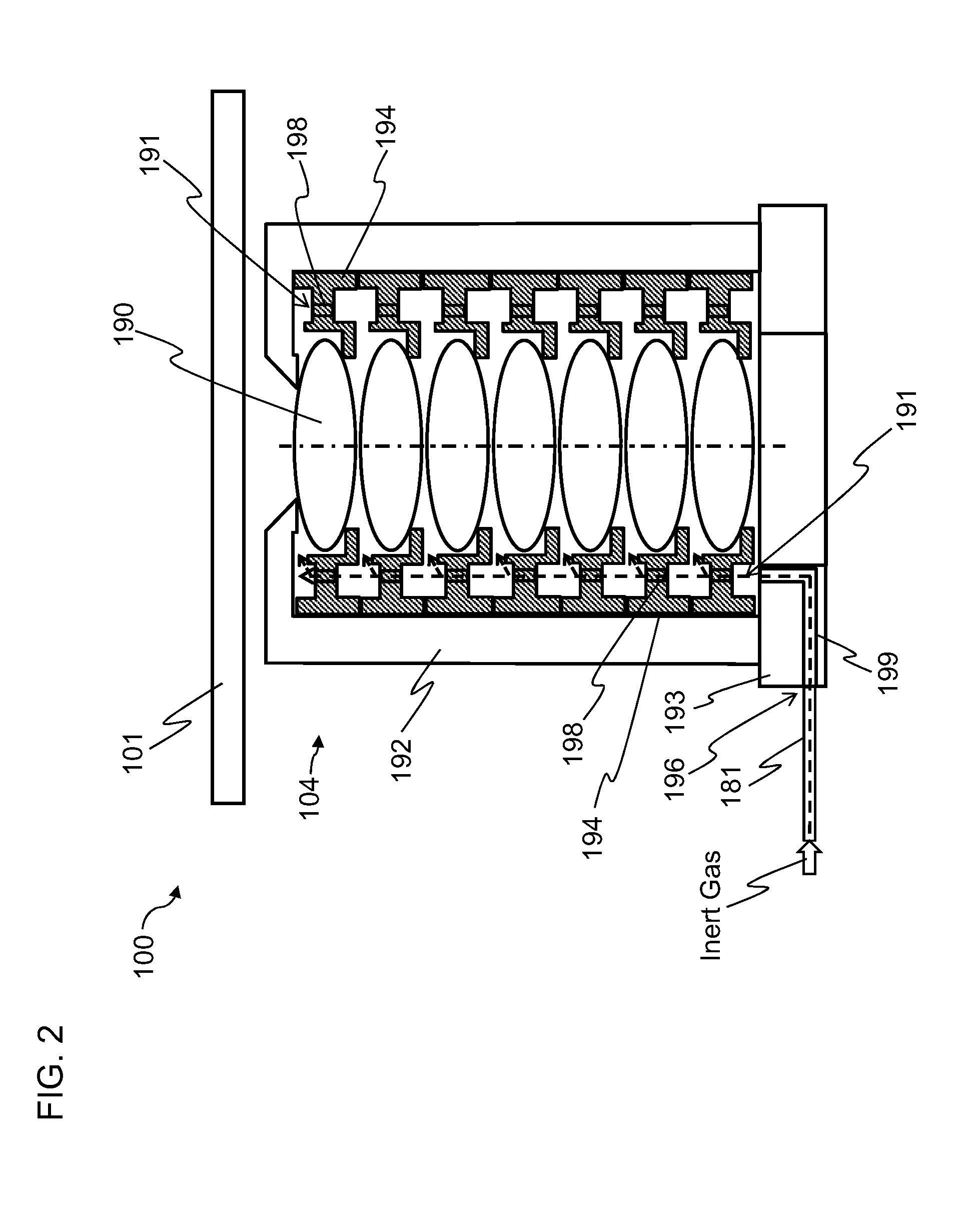
[0125]An inspection apparatus according to the second embodiment of the present invention will be described using the drawings below.

[0126]The inspection apparatus according to the second embodiment of the invention includes the configuration unit A in which the optical image is acquired, similar to the configuration unit A of the above-mentioned inspection apparatus100 according to the first embodiment, and the configuration unit B in which the processes necessary for the inspection are performed using the optical image acquired in the configuration unit A, similar to the configuration unit B of the above-mentioned inspection apparatus 100 according to the first embodiment. Further, a gas pipe is included as an example of the gas supply unit, which supplies the inert gas to the objective lens unit of the configuration unit A. The inspection apparatus according to the second embodiment has the same structure as the above-mentioned inspection apparatus 100 according to the first embo...


PUM


Abstract

An inspection apparatus comprising, a light source configured to emit an inspection light, a table configured to mount an inspection target thereon, an illumination optical system configured to direct the inspection light from the light source toward the target, an objective lens unit configured to gather transmitting or reflected light generated after the illumination optical system illuminates the target with the inspection light, a light receiving unit configured to capture an optical image formed from the light illuminated through the objective lens unit, a chamber configured to house the table, light receiving unit, illumination optical system and objective lens unit, a temperature adjustment unit configured to adjust a temperature in the chamber, and a gas supply unit configured to be connected to the objective lens unit to supply an inert gas at a predetermined temperature into the unit.

Description

CROSS-REFERENCE TO THE RELATED APPLICATION[0001]The entire disclosure of the Japanese Patent Application No. 2013-094044, filed on Apr. 26, 2013 including specification, claims, drawings, and summary, on which the Convention priority of the present application is based, are incorporated herein in its entirety.FIELD OF THE INVENTION[0002]The present invention relates to an Inspection Apparatus. With high integration and large capacity of a Large Scale Integration (LSI), a circuit dimension required for a semiconductor element becomes increasingly narrowed. For example, a pattern having a line width of several tens of nanometers is required to be formed in the latest typical logic device.[0003]It is necessary to improve a production yield of the expensive LSI in a production process. In the semiconductor element, during a production process, an original graphic pattern (that is, a mask or a reticle, hereinafter collectively referred to as a mask) in which a circuit pattern is formed i...

Claims


Application Information

Patent Timeline
IPC IPC(8): G01N21/59
CPCG01N21/59G01N21/95607G01N21/956
Inventor TAYA, MAKOTOKIKUIRI, NOBUTAKA
Owner NUFLARE TECH INC
Why Eureka
Try Eureka