Metal bump structure for use in driver IC and method for forming the same

a technology of metal bumps and driver ics, applied in the direction of semiconductor devices, electrical equipment, semiconductor/solid-state device details, etc., can solve the problems of difficult rework of metal bumps made of other metals, such as gold, and serious damage to copper which serves as a metal bump material, etc., to achieve the effect of easy rework

Active Publication Date: 2014-11-06
HIMAX TECH LTD
View PDF16 Cites 12 Cited by
  • Summary
  • Abstract
  • Description
  • Claims
  • Application Information

AI Technical Summary

Benefits of technology

[0008]In the light of the above, the present invention first proposes a metal bump structure for use in an anisotropic conductive film (ACF) bonding or in a driver IC (integrated circuit). This metal bump structure is basically indifferent to the galvanic effect in the presence of extreme or abnormal conditions under the protection of an extremely thin protective layer. Further, this copper bump structure is easy to rework without damaging the reliability of the electronic circuits. In particular, a lateral fringe is formed during a plating process.
[0009]The metal bump structure for use in a driver IC includes a matrix, a metal bump, a cover layer such as an optional capping layer and an optional protective layer. The matrix includes a substrate, a metal pad, a passivation layer and an adhesion layer. The passivation layer is disposed on the metal pad and defines a recess disposed on the metal pad. The adhesion layer is completely disposed in the recess, disposed on the metal pad and partially disposed on the passivation layer so that the adhesion layer is in direct contact with the metal pad and with the passivation layer. The metal bump fills the recess and covers the adhesion layer. The cover layer completely covers the metal bump so that the metal bump is not exposed to an ambient atmosphere. In particular, the cover layer has a fringe which extends in a lateral direction and the fringe is disposed on the passivation layer. The protective layer consists of a layer of gold as thin as possible and is capable of keeping the metal bump away from being exposed to an ambient atmosphere.
[0021]In another embodiment of the present invention, the metal bump structure is free of a galvanic effect in the presence of a high electric field or halogen.
[0037]In another embodiment of the present invention, the metal bump is free of a galvanic effect in the presence of high electric field or halogen.
[0044]In another embodiment of the present invention, the electroless step is carried out to control the growing rate of the protective layer around 0.006 μm / min so that the resultant thickness of the protective layer is as small as possible.

Problems solved by technology

However, in some application cases, copper which serves as a metal bump material suffers serious damages due to an undesirable phenomenon, namely galvanic effect, in the presence of extreme or abnormal conditions.
This is adverse to the electronic circuits.
Further, metal bumps made of other metals, such as gold, are extremely difficult to re-work once the metal bumps are flawed because aqua regia for re-working is a very corrosive chemical agent.
When the electronic circuits with the flawed metal bumps are re-worked anyway, the reliability of the electronic circuits is possibly seriously compromised.

Method used


Image

  • Metal bump structure for use in driver IC and method for forming the same
  • Metal bump structure for use in driver IC and method for forming the same
  • Metal bump structure for use in driver IC and method for forming the same

Examples


Embodiment Construction

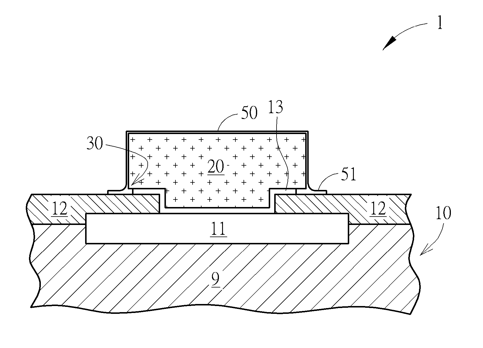
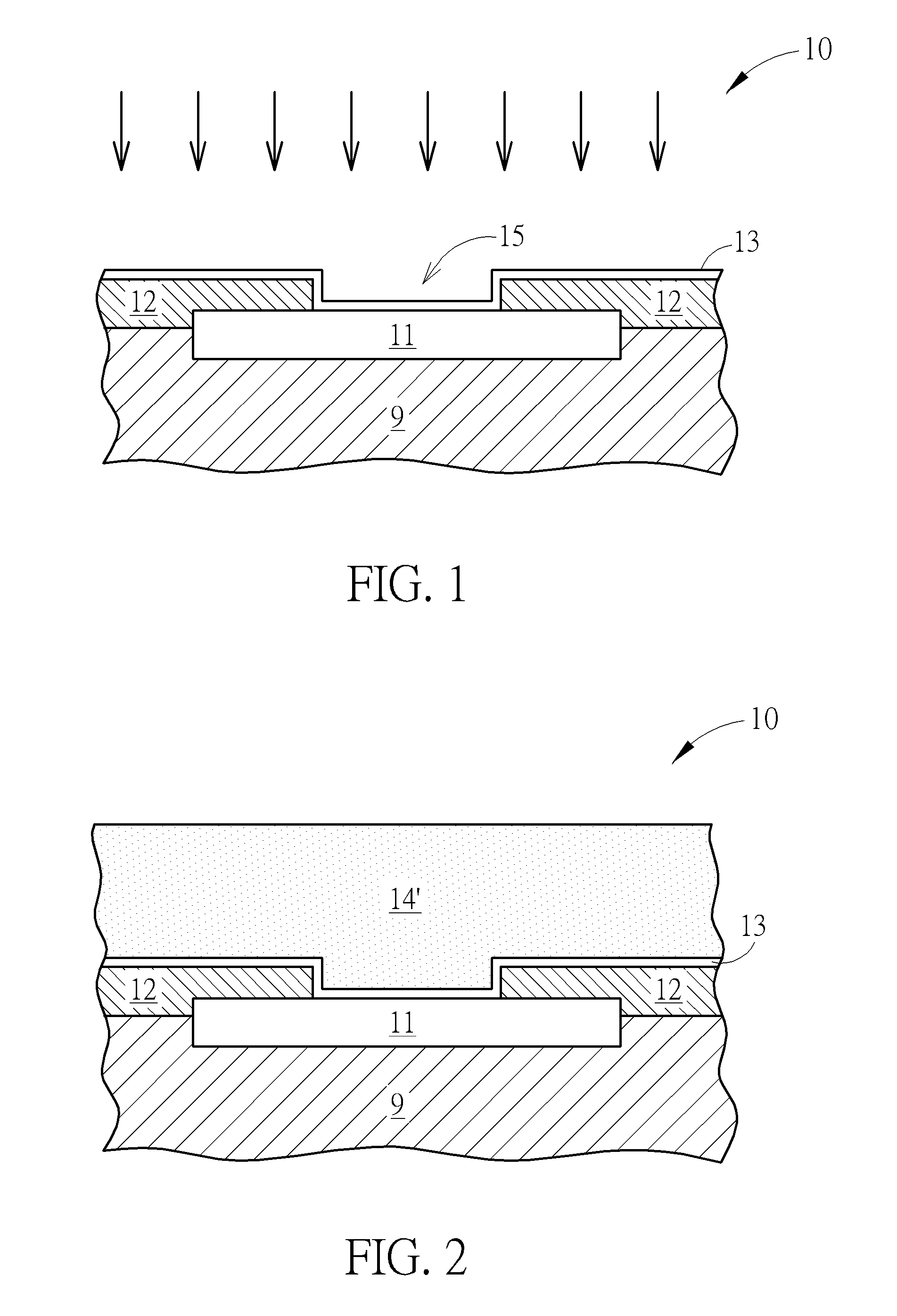
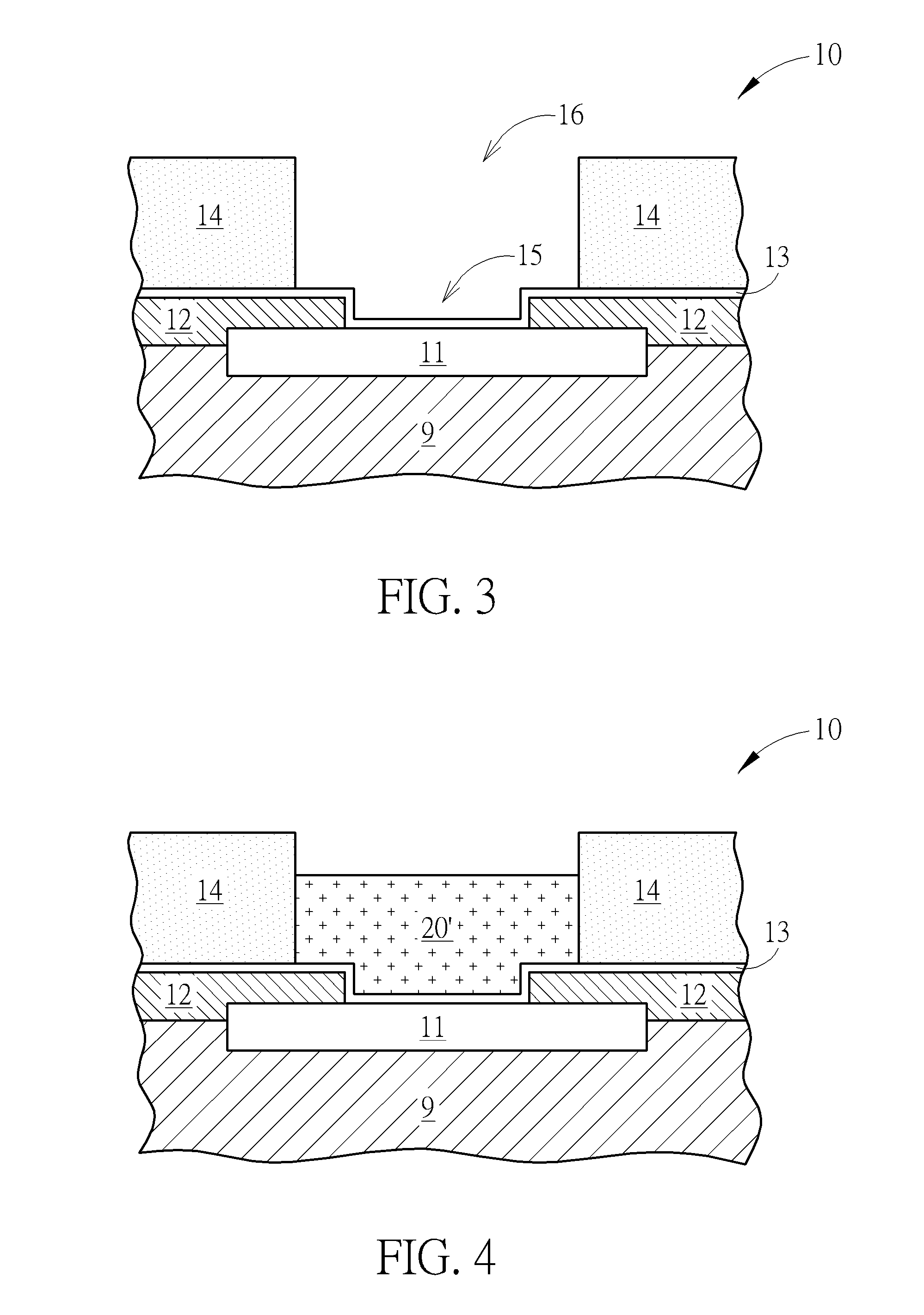
[0049]The present invention first provides a method for forming a metal bump structure for use in a driver IC, in a chip on glass (COG) package or in a chip on flex (COF) package. FIG. 1 to FIG. 6 illustrate a possible method to form the desirable metal bump structure. The metal bump structure may be formed by using a patterned photoresist. The patterned photoresist may be formed as follows. First, please refer to FIG. 1, a substrate 10 is provided. The substrate 10 includes an insulating layer 9, a metal pad 11, a passivation layer 12 and an adhesion layer 13.

[0050]The insulating layer 9 is the basis of the substrate 10 to support other elements, such as the metal pad 11, the passivation layer 12, and the adhesion layer 13 and the patterned photoresist (not shown) formed in a later step. The metal pad 11 may be a light weight material, such as Al, and patterned. However, other metal materials may be suitable as well.

[0051]The passivation layer 12 is disposed on the metal pad 11 and...


PUM

PropertyMeasurementUnit
thicknessaaaaaaaaaa
thicknessaaaaaaaaaa
temperatureaaaaaaaaaa

Abstract

A metal bump structure for use in a driver IC includes a metal bump disposed on a matrix, an optional capping layer disposed on the metal bump to completely cover the metal bump and a protective layer disposed on the metal bump to completely cover and protect the metal bump or the optional capping layer and so that the metal bump is not exposed to an ambient atmosphere. The protective layer or the optional capping layer may have a fringe disposed on the matrix.

Description

CROSS REFERENCE TO RELATED APPLICATIONS[0001]This application claims the benefit of U.S. Provisional Application Ser. No. 61 / 820,152, filed May 6, 2013.BACKGROUND OF THE INVENTION[0002]1. Field of the Invention[0003]The present invention generally relates to a metal bump structure and a method for forming the same. In particular, the present invention is directed to a metal bump structure for use in a driver IC to be protected from an ambient atmosphere, free of a galvanic effect in the presence of high electric field or halogen as well as a method for forming the same.[0004]2. Description of the Prior Art[0005]In some electronic circuits, metal bumps are used to form connections between two groups of circuits. In order to lower the inevitable contact resistance and to achieve the best possible results, copper is often used as the first choice of the metal bump material.[0006]Generally speaking, copper is an ideal metal to serve as a metal bump material because it is not chemically ...

Claims


Application Information

Patent Timeline
Patent Type & Authority Applications(United States)
IPC IPC(8): H01L21/768H01L29/43H01L23/00
CPCH01L21/7685H01L24/10H01L24/11H01L29/43H01L2924/01046H01L2224/1147H01L2924/01029H01L2924/01079H01L2224/11825H01L2224/05027H01L2224/03614H01L24/03H01L24/05H01L24/13H01L2224/0345H01L2224/05582H01L2224/05647H01L2224/1146H01L2224/1181H01L2224/13139H01L2224/13144H01L2224/13147H01L2224/13164H01L2224/13552H01L2224/13562H01L2224/1357H01L2224/13582H01L2224/13611H01L2224/13644H01L2224/13655H01L2224/13664H01L2224/03912H01L2224/13006H01L2224/11848H01L2224/05572H01L2924/15788H01L2224/0401H01L2224/05009H01L2224/05022H01L2224/05124H01L2224/05166H01L2224/1134H01L2224/0361H01L2224/1182H01L2924/00014H01L2924/00012H01L2924/00H01L2924/01074H01L2924/01028H01L2924/0105
Inventor LIN, CHIU-SHUN
Owner HIMAX TECH LTD
Why Eureka
Try Eureka