Semiconductor package having EMI shielding function and heat dissipation function

Active Publication Date: 2014-11-06
SAMSUNG ELECTRONICS CO LTD
View PDF0 Cites 13 Cited by
  • Summary
  • Abstract
  • Description
  • Claims
  • Application Information

AI Technical Summary

Benefits of technology

[0008]Embodiments of the present general inventive concept provide a semiconductor package in which e

Problems solved by technology

Electromagnetic interference (EMI) is generated due to interference between different types of signals in a semiconductor packag

Method used


Image

  • Semiconductor package having EMI shielding function and heat dissipation function
  • Semiconductor package having EMI shielding function and heat dissipation function
  • Semiconductor package having EMI shielding function and heat dissipation function

Examples


Embodiment Construction

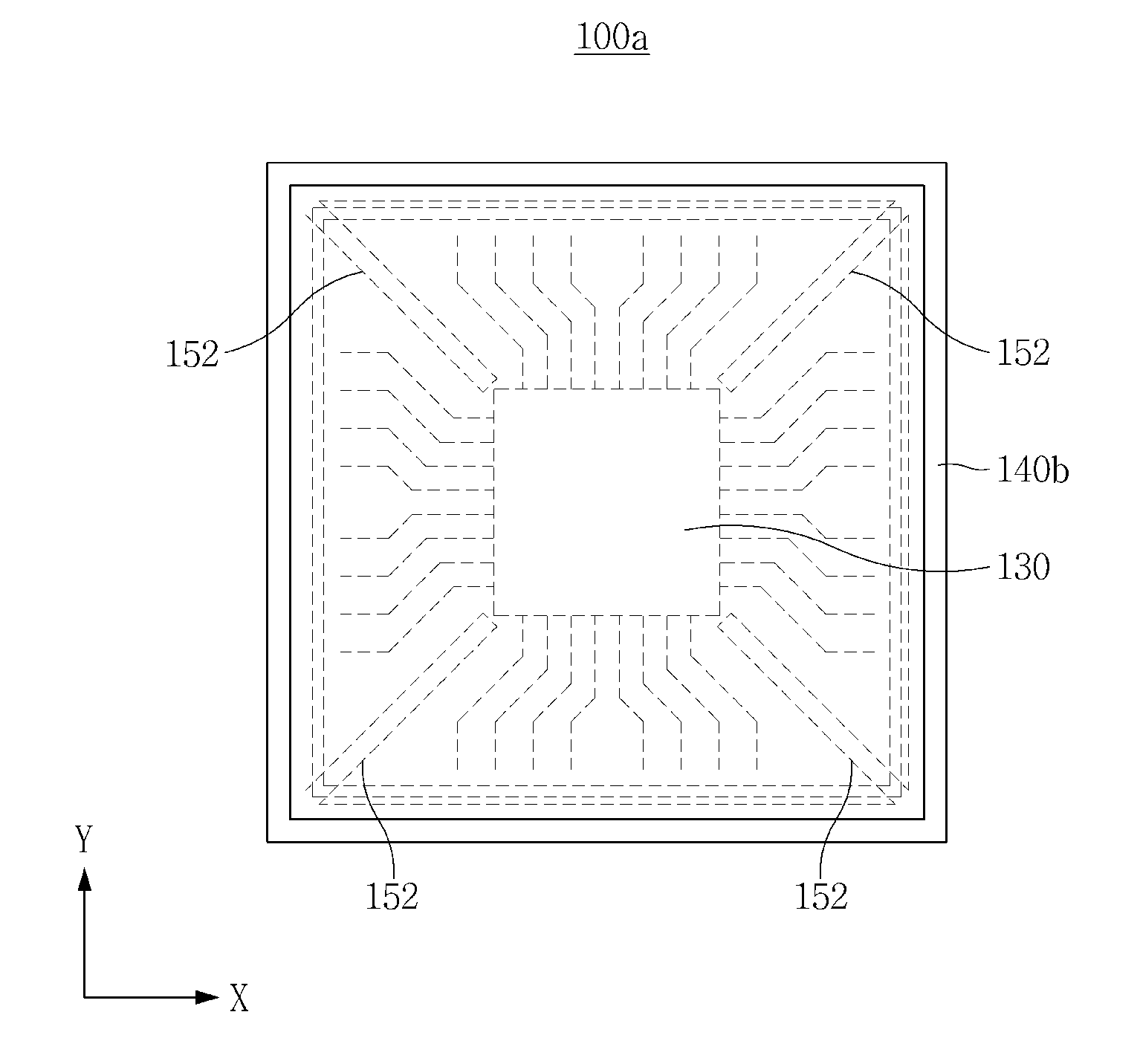
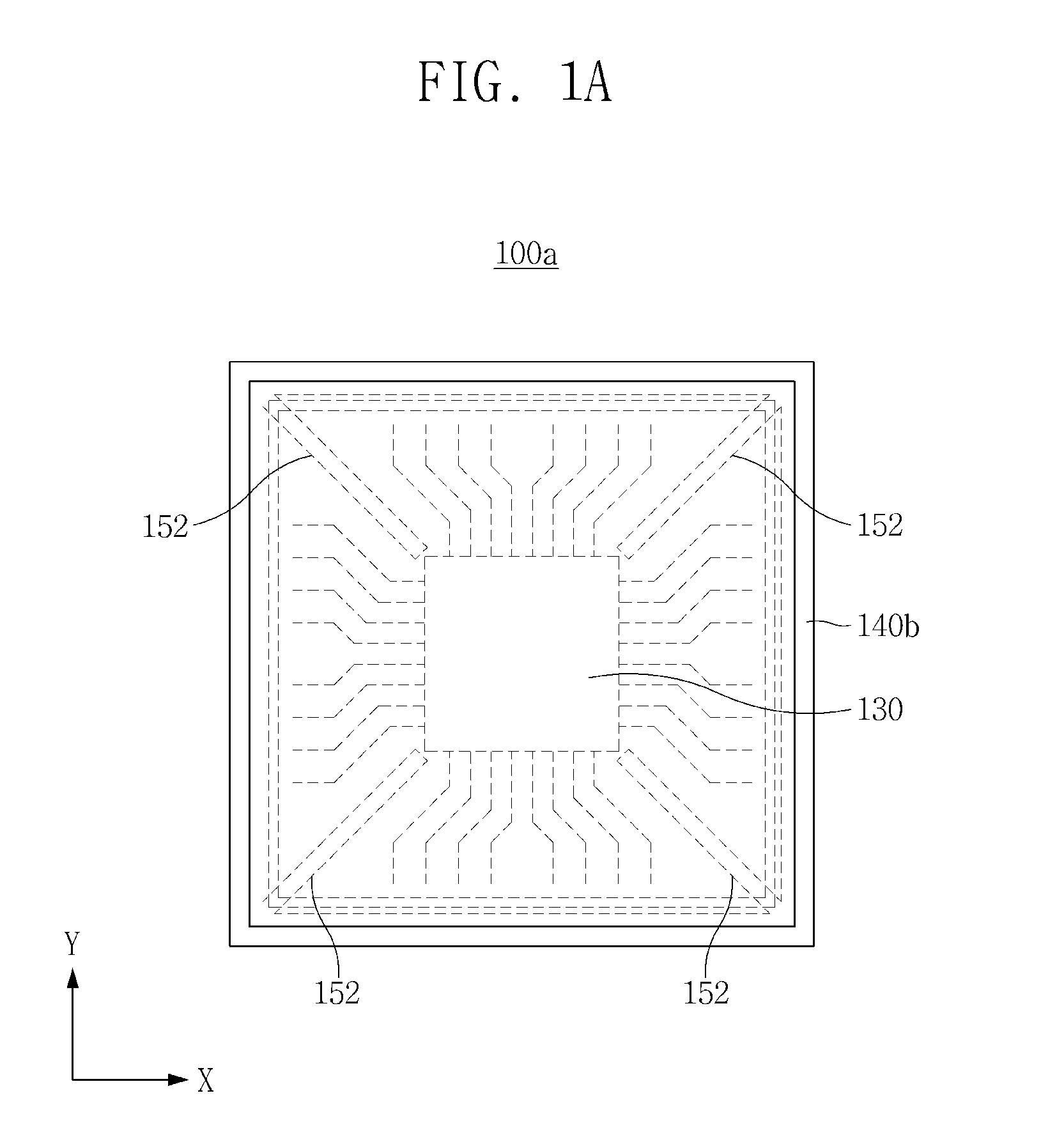
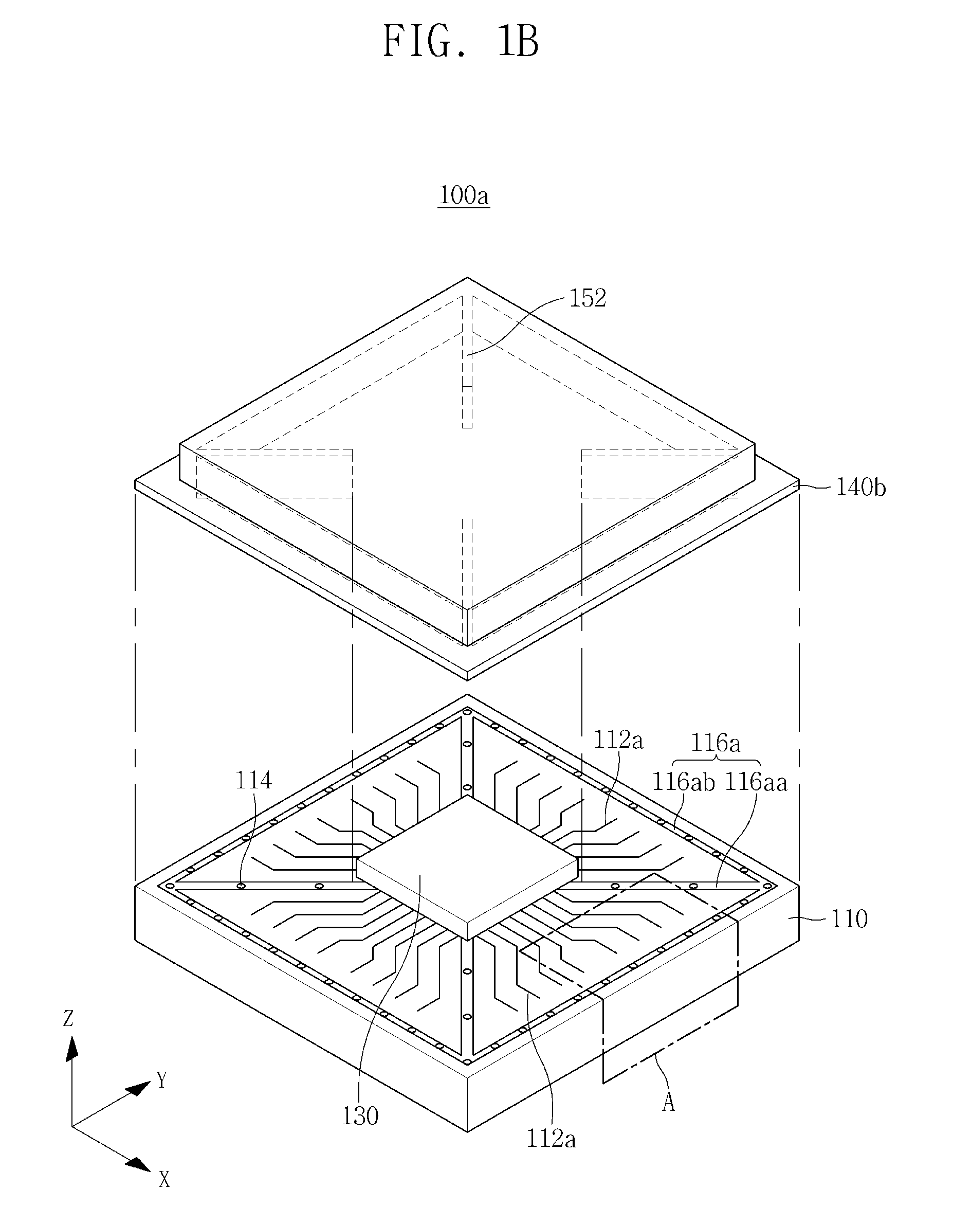
[0051]The features and objectives of the present general inventive concept will become more apparent through the following embodiments and drawings. The embodiments are provided so that this disclosure will be thorough and complete and will fully convey the scope of the inventive concept to one of ordinary skill in the art. Accordingly, the present general inventive concept may be embodied in many different forms and should not be construed as limited to the exemplary embodiments set forth herein. In the drawings, shapes and sizes of layers and regions are intended to assist the understanding of the inventive concept and may be exaggerated for convenience. Thus, the regions illustrated in the figures are schematic in nature and their shapes are not intended to illustrate the actual shapes of regions and are not intended to limit the scope of the present general inventive concept. The same reference numerals used herein denote the same elements.

[0052]Reference will now be made in det...


PUM


Abstract

A semiconductor package includes a substrate, a semiconductor chip located on a top surface of the substrate, signal lines formed on the top surface of the substrate and configured to allow different types of signals to input/output thereto/therefrom, a ground line unit formed on the top surface of the substrate and configured to divide the signal lines into signal lines to/from which the same types of signals are input/output to be isolated from one another, barrier walls configured to contact the ground line unit, and a heat dissipation unit disposed on the semiconductor chip, wherein the ground line unit includes diagonal ground lines located in diagonal directions of the substrate about the semiconductor chip, and the heat dissipation unit includes a thermal interface material (TIM) located on a top surface of the semiconductor chip, and a heat dissipation plate configured to cover the TIM and the substrate.

Description

CROSS-REFERENCE TO RELATED APPLICATIONS[0001]This application claims the benefit of priority under 35 U.S.C. §119 to Korean Patent Application No. 10-2013-0049495 filed on May 2, 2013, the disclosure of which is hereby incorporated by reference in its entirety.BACKGROUND[0002]1. Field[0003]Embodiments of the present general inventive concept relate to a semiconductor package that may shield electromagnetic interference (EMI) generated due to interference between different types of signals, and may discharge heat generated therein.[0004]2. Description of the Related Art[0005]Lately, for mobile products, a multifunctional chip is required not only to have a thin design with a uniform thickness but also to integrate functional chips into one chip in order to minimize areas occupied by the functional chips.[0006]Electromagnetic interference (EMI) is generated due to interference between different types of signals in a semiconductor package including such multi-functional semiconductor c...

Claims


Application Information

Patent Timeline
IPC IPC(8): H01L23/552
CPCH01L23/552H01L24/13H01L24/16H01L24/29H01L24/32H01L24/73H01L2224/131H01L2224/16225H01L2224/2929H01L2224/29339H01L2224/29387H01L2224/29388H01L2224/32225H01L2224/32245H01L2224/73204H01L2224/73253H01L2924/15192H01L2924/15311H01L2924/1615H01L2924/16251H01L2924/16747H01L2924/16724H01L2924/00012H01L2924/014H01L2924/00H05K9/00H01L23/60
Inventor CHOI, IN-HOKIM, YONG-HOONSHIN, SEONG-HO
Owner SAMSUNG ELECTRONICS CO LTD
Why Eureka
Try Eureka