Method for manufacturing nanostructures and cathode for field emission lighting arrangement

a manufacturing method and technology for cathode, applied in the manufacture of electrode systems, discharge tube main electrodes, electric discharge tubes/lamps, etc., can solve the problems of inconvenient large-scale fabrication, complex and expensive recycling of fluorescent light sources, and inconvenient process steps

Active Publication Date: 2014-11-27
PUREFIZE TECH AB
View PDF5 Cites 9 Cited by
  • Summary
  • Abstract
  • Description
  • Claims
  • Application Information

AI Technical Summary

Benefits of technology

[0006]In view of the above-mentioned and other drawbacks of the prior art, a general object of the present invention is to provide an improved method for fabricating nanostructures suitable for use as field emitters.

Problems solved by technology

However, LED devices are expensive and complicated to fabricate and fluorescent light sources are known to contain small amounts of mercury, thereby posing potential health problems due to the health risks involved in mercury exposure.
Furthermore, as a result of the mercury content, recycling of fluorescent light sources is both complicated and costly.
However, the method disclosed by Yang et al. includes several process steps not suitable for large scale fabrication of field emission devices such as the high temperature growth step and the random distribution of nanostructures.

Method used


Image

  • Method for manufacturing nanostructures and cathode for field emission lighting arrangement
  • Method for manufacturing nanostructures and cathode for field emission lighting arrangement
  • Method for manufacturing nanostructures and cathode for field emission lighting arrangement

Examples


Embodiment Construction

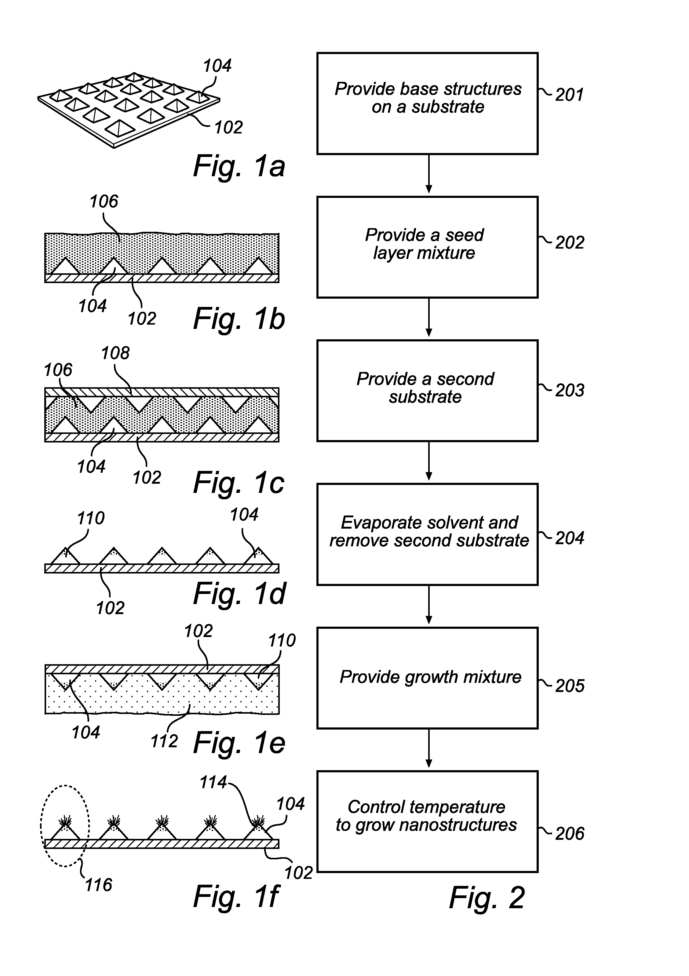
[0039]In the present detailed description, various embodiments of a method for fabricating nanostructures according to the present invention are mainly discussed with reference to ZnO nanostructures suitable for use as field emitters. It should be noted that this by no means limits the scope of the present invention which is equally applicable to nanostructures comprising other materials. Like reference characters refer to like elements throughout.

[0040]A method according to various embodiments of the present invention will now be described with reference to the flow-chart shown in FIG. 2 outlining the general method steps for fabrication of nanostructures together with FIGS. 1a to 1f illustrating the nanostructure device in different stages of the manufacturing process.

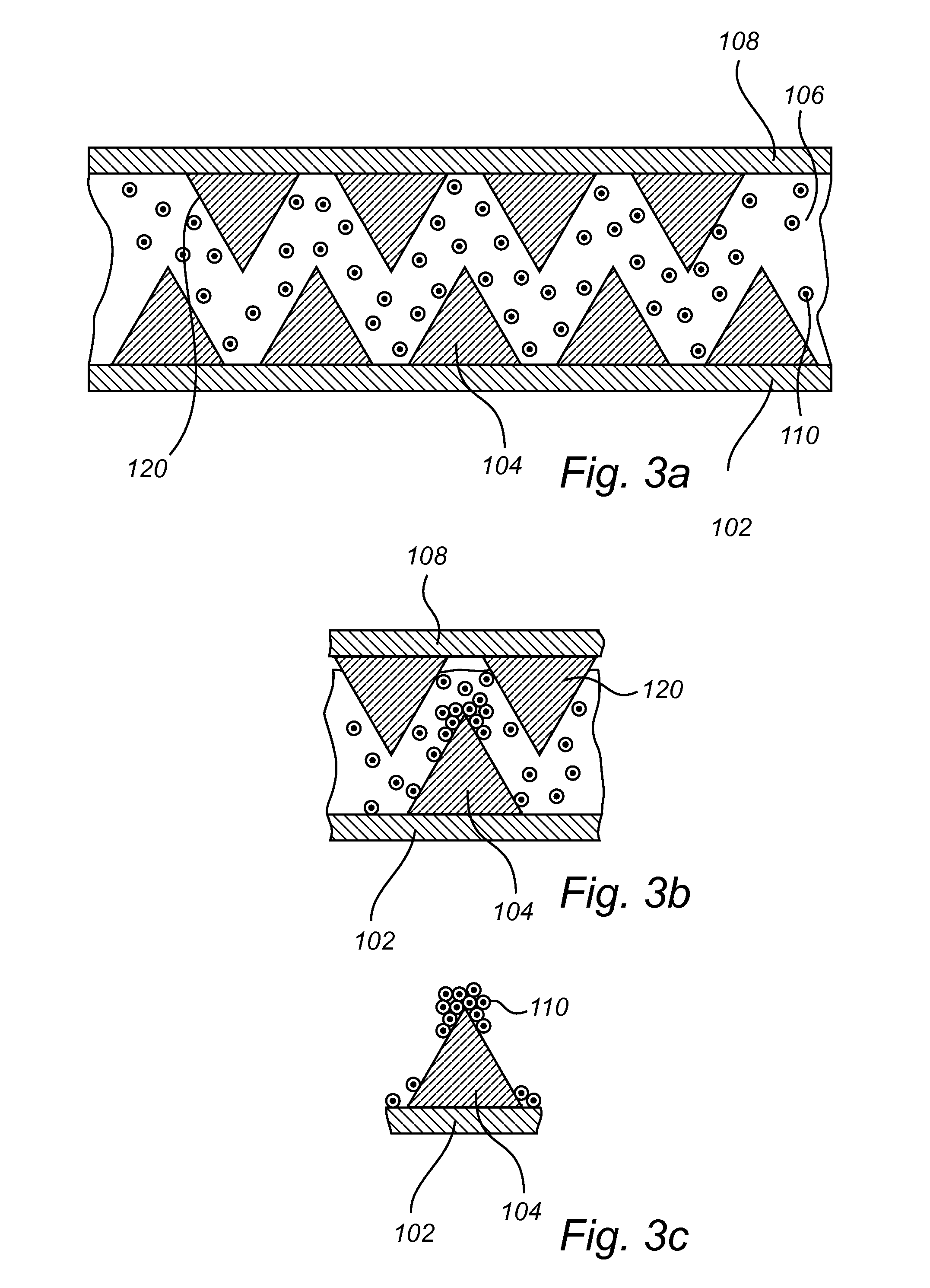
[0041]First, in step 201 illustrated in FIG. 1a, a preferred substrate 102 comprising pyramid shaped protruding base structures 104 is provided. The substrate can be of any insulating, semiconducting or conducting su...


PUM

PropertyMeasurementUnit
temperatureaaaaaaaaaa

Abstract

The present invention relates to a method for manufacturing a plurality of nanostructures comprising the steps of providing a plurality of protruding base structures (104) arranged on a surface of a first substrate (102), providing a seed layer mixture, comprising a solvent / dispersant and a seed material, in contact with the protruding base structures, providing a second substrate arranged in parallel with the first substrate adjacent to the protruding base structures, thereby enclosing a majority of the seed layer mixture between the first and second substrates, evaporating the solvent, thereby forming a seed layer (110) comprising the seed material on the protruding base structures, removing the second substrate, providing a growth mixture, comprising a growth agent, in contact with the seed layer, and controlling the temperature of the growth mixture so that nanostructures (114) are formed on the seed layer via chemical reaction in presence of the growth agent.

Description

FIELD OF THE INVENTION[0001]The present invention relates to a method for fabricating nanostructures on a substrate. The present invention also relates to a cathode, to be used in a field emission arrangement, comprising nanostructures.TECHNICAL BACKGROUND[0002]Traditional incandescent light bulbs are currently being replaced by other light sources having higher energy efficiency and less environmental impact. Alternative light sources include light emitting diode (LED) devices and fluorescent light sources. However, LED devices are expensive and complicated to fabricate and fluorescent light sources are known to contain small amounts of mercury, thereby posing potential health problems due to the health risks involved in mercury exposure. Furthermore, as a result of the mercury content, recycling of fluorescent light sources is both complicated and costly.[0003]An attractive alternative light source has emerged in the form of field emission light sources. A field emission light sou...

Claims


Application Information

Patent Timeline
Patent Type & Authority Applications(United States)
IPC IPC(8): H01J1/304H01J1/36H01J63/02C30B7/10
CPCH01J1/304C30B7/10C30B29/16H01J63/02H01J1/36H01J1/3044H01J9/025H01J63/04H01J2201/30496
Inventor HU, QIU-HONGYANG, SHANG-RAYBOHLIN, KJELL
Owner PUREFIZE TECH AB
Why Eureka
Try Eureka