
Liquid crystal display device

a liquid crystal display and display device technology, applied in non-linear optics, instruments, optics, etc., can solve the problems of light leakage problem, spacer dislocation, adverse effect of liquid crystal display panel light efficiency, etc., and achieve the effect of improving light transmission ra

Inactive Publication Date: 2014-11-27
AU OPTRONICS CORP
View PDF4 Cites 12 Cited by
  • Summary
  • Abstract
  • Description
  • Claims
  • Application Information

AI Technical Summary

Benefits of technology

The present invention is a liquid crystal display device with a spacer structure between substrates that improves light transmission and solves the issue of light leakage caused by depression.

Problems solved by technology

As such, light efficiency of the liquid crystal panel is adversely affected.
Moreover, when the liquid crystal display is unintentionally depressed, the spacers are likely dislocated due to the depression force.
Meanwhile, the spacers might scratch and damage the alignment layer disposed on top of the array or color filter substrate, and thus lead to a light leakage problem as the liquid crystal molecules could not be aligned at the scratch damage area.

Method used


Image

  • Liquid crystal display device
  • Liquid crystal display device
  • Liquid crystal display device

Examples


first embodiment

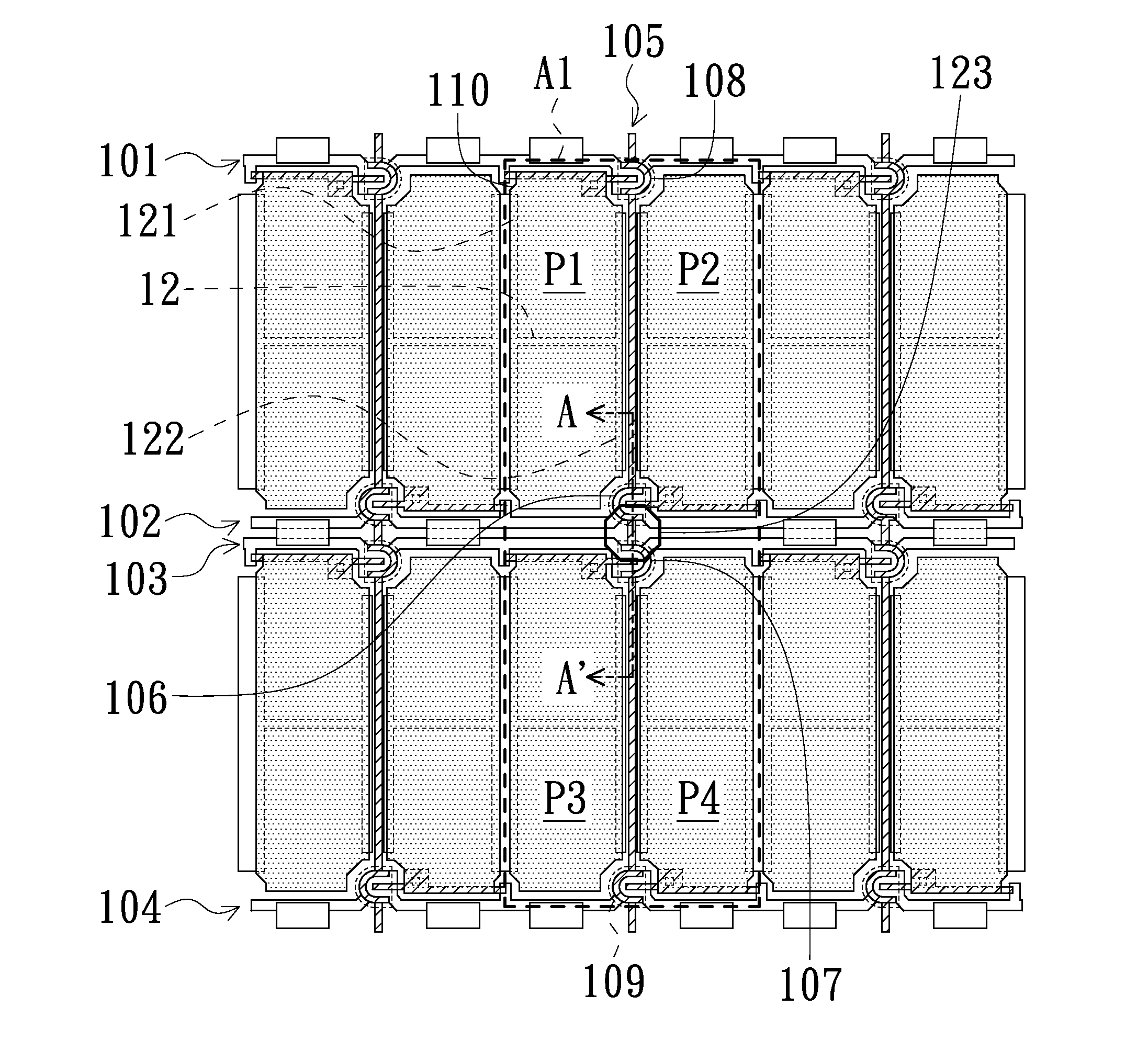
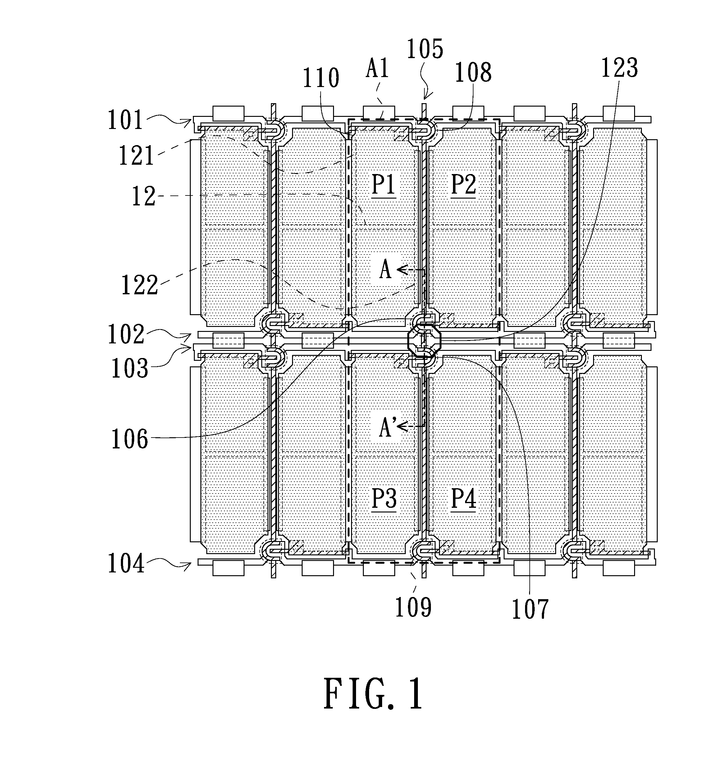
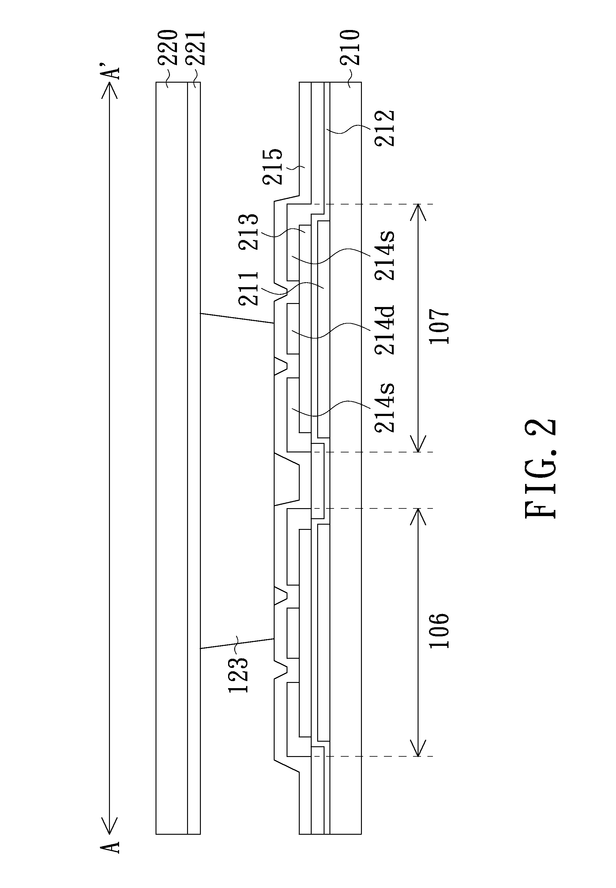
[0017]In this invention, a spacer structure included in a Half Source Driver liquid crystal display is illustrated with reference to FIG. 1, a diagram showing a pixel area of the Half Source Driver LCD device, and FIG. 2, a cross-sectional view of the LCD device of FIG. 1 taken along line A-A′. The area A1 enclosed with the dash line as shown in FIG. 1 is defined as a pixel unit which is composed of four pixels, P1, P2, P3, and P4. These four pixels share a single data line 105 and are respectively driven through a first gate line 101, a second gate line 102, a third gate line 103, and a fourth gate line 104, based on the Half Source Driver structure. The operation of the first pixel P1 is taken as an example. The pixel P1 is disposed on an array substrate and comprises a switch device, which is, for example, a thin film transistor (TFT) 108 as shown in FIG. 1. The TFT 108 is turned on by the gate line 101 first, and then the display signal, or pixel voltage, from the data line 105 ...

second embodiment

[0022]In this invention, the spacer structure is implemented with another type of Half Source Driver liquid crystal display. As shown in FIG. 4, area A2 enclosed with the dash line is defined as a pixel unit, which is composed of eight pixels, P5, P6, P7, P8, P9, PA, PB, and PC. Based on the Half Source Driver structure, the data signal which is written to pixels P5, P6, PB, and PC is supplied by a data line 425, that written to pixels P9 and PA is supplied by a data line 405, and that written to pixels P7 & P8 is supplied by a data line 435. The eight pixels are driven by a first gate line 401, a second gate line 402, a third gate line 403, and a fourth gate line 404, respectively. Each of the pixels P6 and P9 which are disposed on an array substrate comprises one switch device, TFT 406 or TFT 407. The TFTs 406 and 407 are respectively turned on by the gate lines 402 and 403 first, and then the display signals or pixel voltages from a data line branch 425a of the data line 425 and ...

third embodiment

[0024]In this invention, the spacer and the color filter layer structures of the Half Source Driver liquid crystal display are illustrated. As shown in FIG. 5, a schematic diagram of a color filter substrate and an array substrate, the light shielding layer 115 is used to shield the area where liquid crystal molecules are not under control of the pixel voltage, so the light shielding area is required to overlap with the pixel area without pixel electrode, for example, the area of the gate line, the data line, and the thin film transistor. The color filter layer repeats in the order of red, green, and blue along the horizontal direction in FIG. 5. From the schematic diagram of the color filter layer and pixels, the color filter layers cover the light transmission area so the output light from each pixel is transformed to the wavelength corresponding to each color filter layer. The schematic enlarged diagram is represented in FIG. 6 to show the spacer-surrounding area of area C1 in FI...


PUM

PropertyMeasurementUnit
conductiveaaaaaaaaaa
pressureaaaaaaaaaa
light transmission areaaaaaaaaaaa

Abstract

A liquid crystal display device includes a first substrate, a second substrate, and a plurality of spacers. The first substrate includes a plurality of pixel units, which include at least two gate lines, and two neighboring thin film transistors connected to two gate lines, respectively. The second substrate is opposed to the first substrate. At least one of the spacers overlaps with at least a part of the first thin film transistor and at least a part of the second thin film transistor in a top view.

Description

FIELD OF THE INVENTION[0001]The present invention relates to a display device, and more particularly to a liquid crystal display device.BACKGROUND OF THE INVENTION[0002]A liquid crystal display (LCD) panel includes an array substrate, a color filter substrate, and a liquid crystal layer interposed between the array substrate and the color filter substrate. A plurality of spacers are disposed between two substrates of the liquid crystal panel to maintain a cell gap between the array substrate and the color filter substrate and to sustain external pressure exerted on the substrates. For implementing such construction, a light shielding layer above the spacers is required to shield the randomly scattered light resulting from the uncontrolled liquid crystal molecules around the spacers. The disposition of the light shielding layer above the spacers would reduce light transmission area of pixels. As such, light efficiency of the liquid crystal panel is adversely affected.[0003]Moreover, ...

Claims


Application Information

Patent Timeline
Patent Type & Authority Applications(United States)
IPC IPC(8): G02F1/1339
CPCG02F1/1339G02F1/133512G02F1/13394G02F1/1368
Inventor WANG, CHUN-MINSHEN, CHUNG-MINLIN, JIAN-HONG
Owner AU OPTRONICS CORP
Learn More