
OLED Panel, Manufacturing Method, and Related Testing Method

Inactive Publication Date: 2014-12-04
TCL CHINA STAR OPTOELECTRONICS TECH CO LTD
View PDF6 Cites 6 Cited by
  • Summary
  • Abstract
  • Description
  • Claims
  • Application Information

AI Technical Summary

Benefits of technology

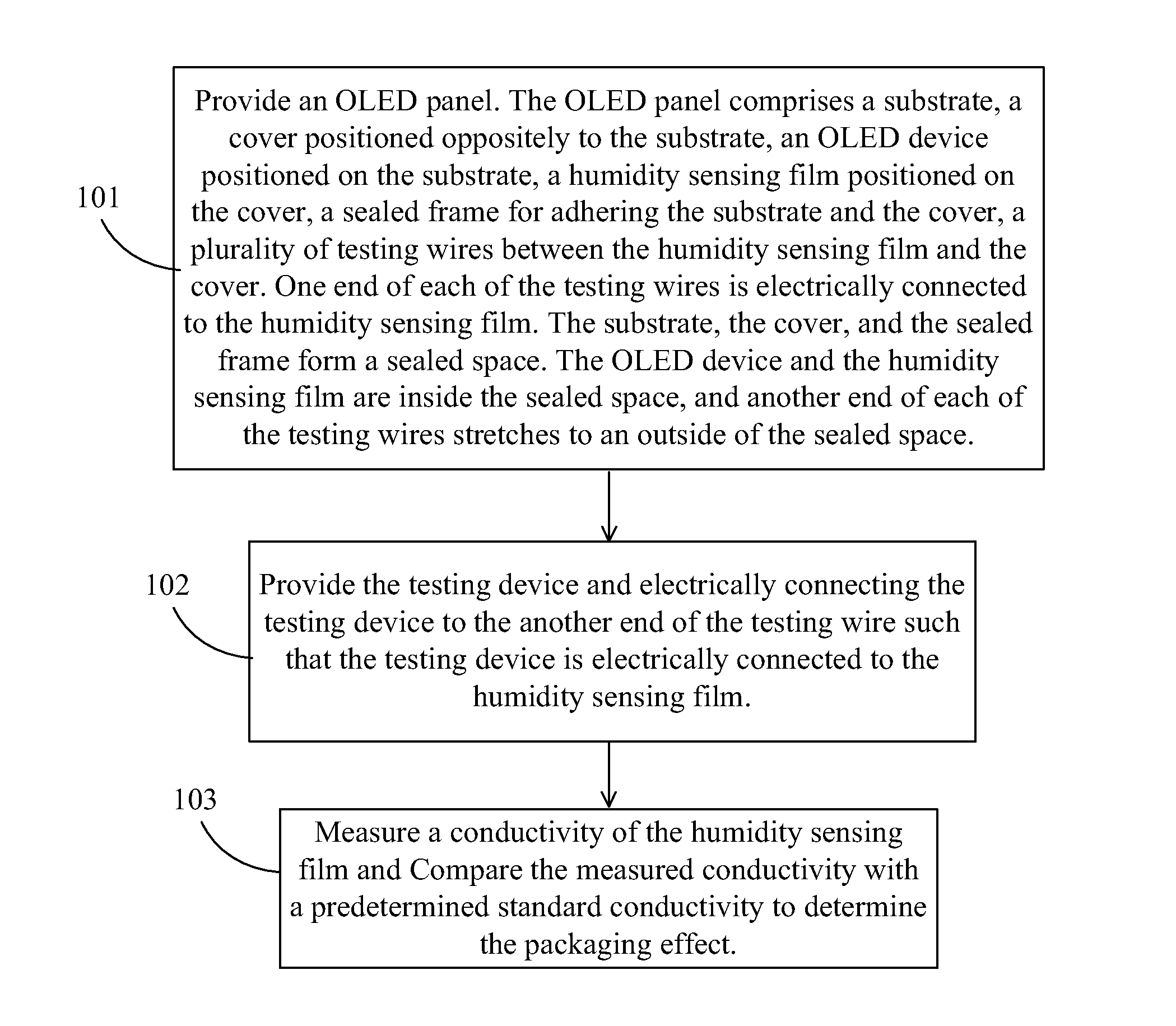
The present invention provides an OLED panel, a manufacturing method, and a testing method that can improve its packaging effect and longer life time. The manufacturing method is simple and can manufacture an OLED panel with a longer life time. The testing method can detect the contained water and oxygen inside the package of the OLED panel, which is easy to accomplish without any side effects on the panel. The invention utilizes a humidity sensing film, which is manufactured with a conductive powder and a high molecular material having a characteristic of easily absorbing humidity to expand. This can be utilized as a desiccant to expand the life time of the OLED panel. The manufacturing method is simple and easy to accomplish.

Problems solved by technology

Flat displays are widely used because they're thin and low power consuming without any radiation.
Therefore, packaging requirements of the OLED displays are very restricted.
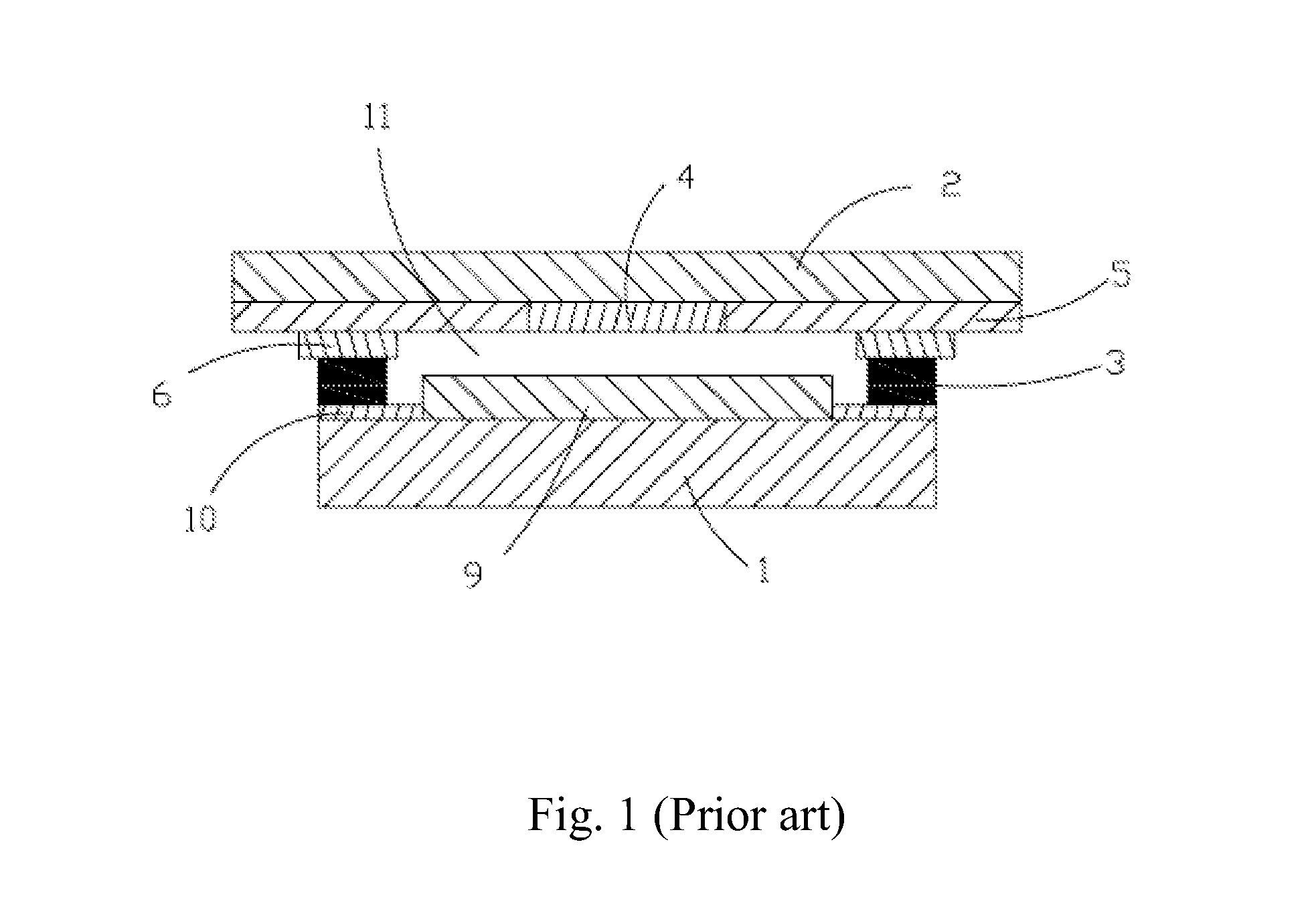
However, according to the current OLED panel manufacturing procedure, very few testing method for testing the packaging effect are introduced.
This method is quite simple, but reliability problem exists.
Furthermore, through compare the photos taken by the camera cannot reflect to a tiny volume difference.
Therefore, this testing method is not good enough and should be improved.
The above-mentioned testing method can test the packaging effect of OLED panel more efficiently, but the manufacturing procedure of the above-mentioned device is more complicated and costs more.
This makes the entire structure of the OLED panel more complicated, and the manufacturing procedures become more complicated correspondingly.

Method used


Image

  • OLED Panel, Manufacturing Method, and Related Testing Method
  • OLED Panel, Manufacturing Method, and Related Testing Method
  • OLED Panel, Manufacturing Method, and Related Testing Method

Examples


Embodiment Construction

[0031]The drawings illustrate embodiments of the invention and, together with the description, serve to explain the principles of the invention.

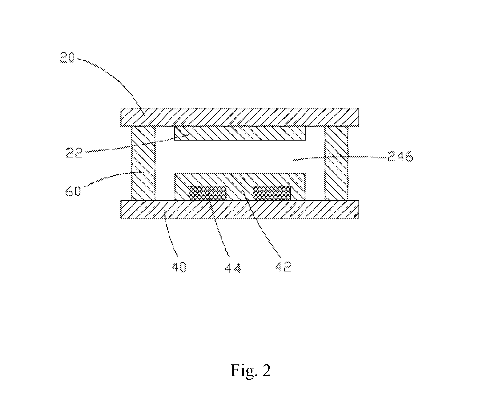
[0032]Please refer to FIG. 2 in conjunction with FIG. 3. An OLED panel is provided. The OLED panel comprises a substrate 20, a cover 40 positioned oppositely to the substrate 20, an OLED device 22 positioned on the substrate 20, a humidity sensing film 42 positioned on the cover 40, and a sealed frame 60 for adhering the substrate 20 and the cover 40. The substrate 20, the cover 40, and the sealed frame 60 form a sealed space 246. The OLED device 22 and the humidity sensing film 42 are both sealed inside the sealed space 246. A plurality of testing wires 44 are positioned between the humidity sensing film 42 and the cover 40. One end of each of the testing wires 44 is electrically connected to the humidity sensing film 42, and another end of each of the testing wires 44 stretches to an outside of the sealed space 246 via the sealed frame 60 ...


PUM


Abstract

The present invention discloses an OLED panel, a manufacturing method and related testing method. The OLED panel includes a substrate (20), a cover (40) positioned oppositely to the substrate (20), an OLED device positioned on the substrate (20), a humidity sensing film (42) positioned on the cover (40), a sealed frame (60) for adhering the substrate (20) and the cover (40), a plurality of testing wires between the humidity sensing film (42) and the cover (40), wherein one end of each of the testing wires is electrically connected to the humidity sensing film (42); wherein the substrate (20), the cover (40), and the sealed frame (246) form a sealed space, the OLED device and the humidity sensing film (42) are inside the sealed space, and another end of each of the testing wires stretches to an outside of the sealed space (246).

Description

BACKGROUND OF THE INVENTION[0001]1. Field of the Invention[0002]The invention relates to a flat display, and more particularly, to an OLED panel, related manufacturing method, and related testing method for testing its packaging effect.[0003]2. Description of the Prior Art[0004]Flat displays are widely used because they're thin and low power consuming without any radiation. The flat displays include liquid crystal displays (LCD) and organic light emitting displays (OLED).[0005]The OLED displays have characteristics of self-lighting, high-luminance, wide view angle, high contrast, bendable figure, low power consumption. Therefore, OLED displays are regarded as a new generation of displays, and gradually replace the traditional LCD displays. The OLED displays are widely utilized as cell phone screens, computer monitors, and TV screens. The display mechanisms of the OLED and LCD are different. OLED displays do not need any backlight module, instead, OLED displays adopt very thin organi...

Claims


Application Information

Patent Timeline
IPC IPC(8): H01L27/32H01L21/66H01L51/56
CPCH01L27/3225H01L22/30H01L22/12H01L51/56G09G3/006G09G3/3208G09G2300/0421G09G2330/12H10K59/00H10K71/70H10K50/841H10K50/846
Inventor ZENG, WEIJING
Owner TCL CHINA STAR OPTOELECTRONICS TECH CO LTD
Learn More