Substrate for use in manufacturing display device and method for forming element on substrate

Active Publication Date: 2014-12-04
SAMSUNG DISPLAY CO LTD
View PDF4 Cites 22 Cited by
  • Summary
  • Abstract
  • Description
  • Claims
  • Application Information

AI Technical Summary

Benefits of technology

[0045]According to embodiments of the invention, a thin film for a test (or indicator for calibrating alignment) does not overlap an alignment mark, so that a measurement range of a measurement equipment may not be limited by the alignment mark. Accordingly, the measurable range may be maximized, and substantially a

Problems solved by technology

During the deposition process, if an error occurs in the alignment between

Method used


Image

  • Substrate for use in manufacturing display device and method for forming element on substrate
  • Substrate for use in manufacturing display device and method for forming element on substrate
  • Substrate for use in manufacturing display device and method for forming element on substrate

Examples


Example

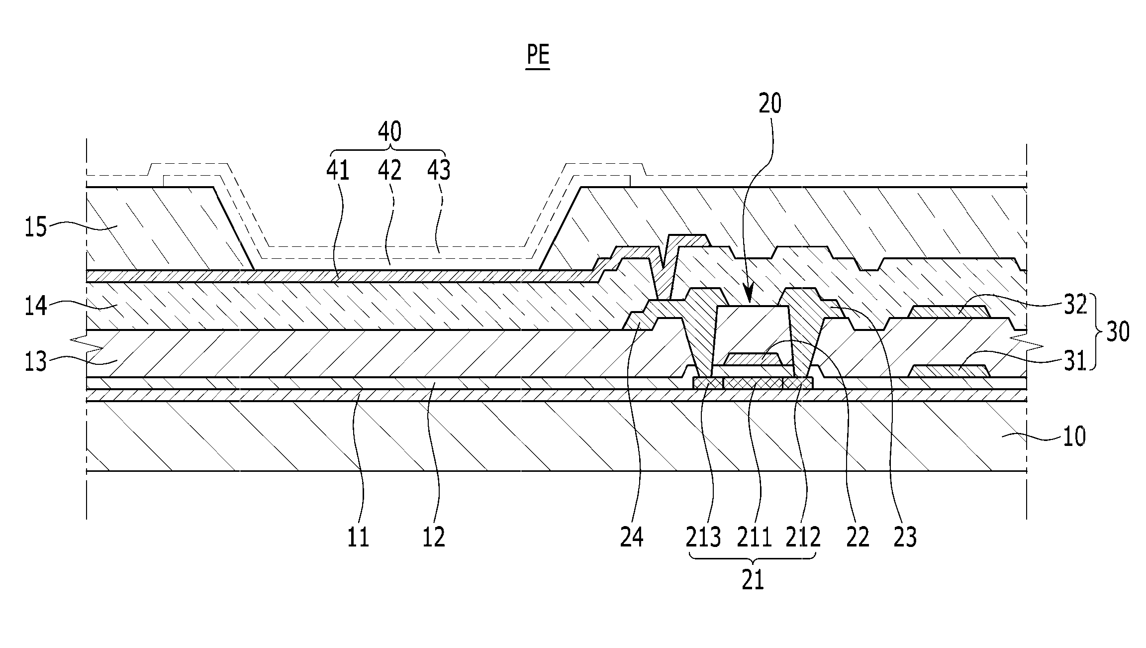
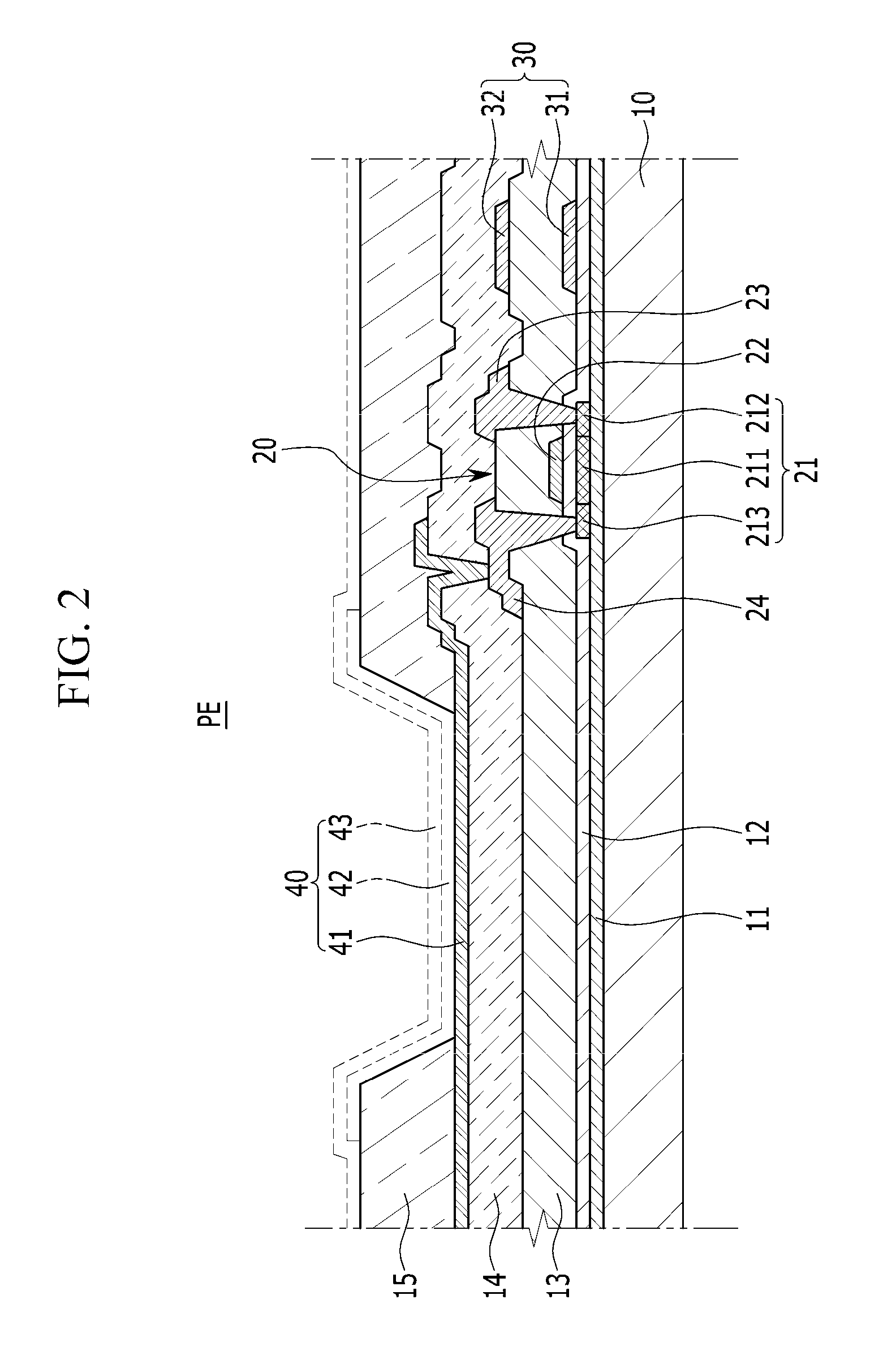
[0056]The present invention is described more fully hereinafter with reference to the accompanying drawings, in which embodiments of the invention are shown. As those skilled in the art would realize, the described embodiments may be modified in various different ways, all without departing from the spirit or scope of the present invention.

[0057]In the description and claims, if a part “includes” a component, the part may further include zero or more additional components. In the description and claims, when it is described that a first element (such as one of a layer, a film, an area, a plate, etc.) is “on” or “above” a second element, it may mean that the first element directly contacts the second element, or it may mean that a third element exists between the first element and the second element.

[0058]Although the terms first, second, etc. may be used herein to describe various signals, elements, components, regions, layers, and / or sections, these signals, elements, components, r...


PUM


Abstract

A substrate is for use in manufacturing a display device. The substrate includes a first area that corresponds to pixel positions. The substrate further includes a second area adjacent to the first area. The substrate further includes a first mark disposed in the second area, wherein a first virtual line corresponds to the first mark. The substrate further includes a second mark disposed in the second area and spaced from the first mark, wherein a second virtual line corresponds to the second mark and intersects the first virtual line at a virtual reference point. The substrate further includes an indicator disposed in the second area, spaced from the first mark and the second mark, and corresponding to an opening of a mask, wherein a positional relation between the virtual reference point and a point of the indicator represents a positional relation between the substrate and the mask.

Description

RELATED APPLICATIONS[0001]This application claims priority to and the benefit of Korean Patent Application No. 10-2013-0062048 filed in the Korean Intellectual Property Office on May 30, 2013, the entire contents of which are incorporated herein by reference.BACKGROUND[0002]1. Field[0003]The present invention relates to a substrate for a display device and a method for depositing a thin film.[0004]2. Description of the Related Art[0005]An organic light emitting display typically includes a substrate and a plurality of pixels formed on the substrate. Each of the pixels includes a pixel circuit and an organic light emitting diode of which emission may be controlled by the pixel circuit. The organic light emitting diode may have a stacked structure that may include a pixel electrode, an organic emission layer, and (a portion of) a common electrode. The organic light emitting display may use lights emitted from a plurality of organic light emitting diodes to display an image.[0006]The o...

Claims


Application Information

Patent Timeline
IPC IPC(8): H01L51/00H01L27/32
CPCH01L27/3246H01L51/0012H01L23/544H01L2223/5442H01L2223/54426H01L2223/54486H01L2924/0002H10K59/35H10K71/10H10K71/00H01L2924/00G09F9/00H10K71/191H10K59/122
Inventor JEONG, CHEOL-GYU
Owner SAMSUNG DISPLAY CO LTD
Why Eureka
Try Eureka