Electrostatic Discharge (ESD) Protection Circuit with EOS and Latch-Up Immunity
- Summary
- Abstract
- Description
- Claims
- Application Information
AI Technical Summary
Benefits of technology
Problems solved by technology
Method used
Image

Examples
first embodiment
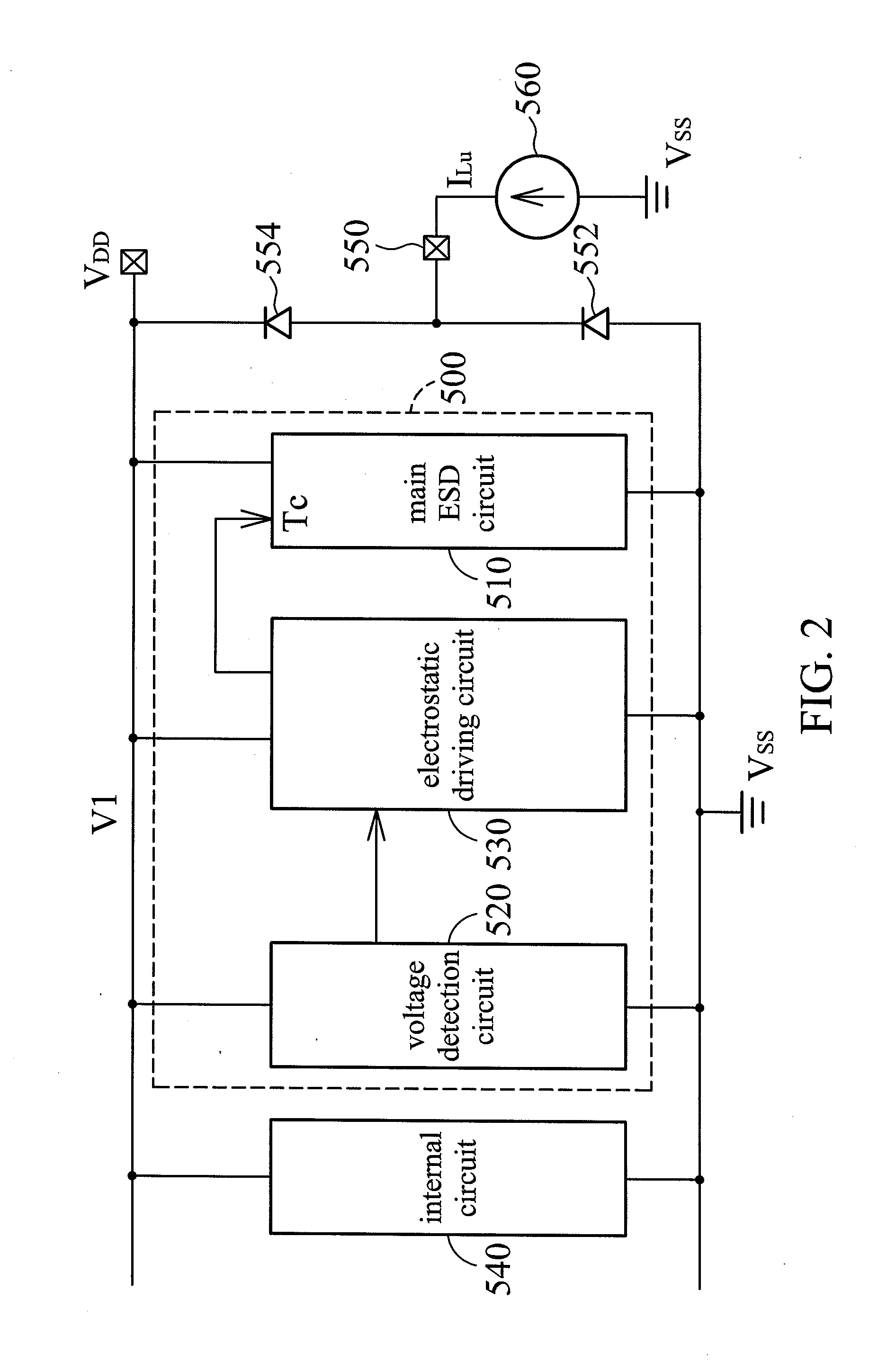
[0030]FIG. 3 is a schematic diagram illustrating the electrostatic discharge protection circuit of FIG. 2 of the present invention. As FIG. 3 shows, the electrostatic discharge protection circuit 600 includes a main ESD circuit 610, a voltage detection circuit 620 and an electrostatic driving circuit 630. The main ESD circuit 610 is configured to establish the electrical connection between the first rail VDD and the second rail VSS based on the voltage at the control end Tc. The voltage detection circuit 620 is arranged to set the voltage at the control end Tc when the voltage V1 at the first rail VDD is greater than the limiting voltage for driving the main ESD circuit 610 to establish the electrical connection between the first rail VDD and second rail VSS. The electrostatic driving circuit 630 is configured to set the voltage at the control end Tc to drive the main ESD circuit 610 to establish the electrical connection between the first rail VDD and the second rail VSS when the i...
second embodiment
[0036]FIG. 6 is a schematic diagram illustrating the electrostatic discharge protection circuit of FIG. 2 of the present invention. As shown in FIG. 6, the electrostatic discharge protection circuit 900 is similar to the electrostatic discharge protection circuit 600 except that the voltage detection circuit 620 of the electrostatic discharge protection circuit 600 is replaced by the voltage detection circuit 920 of the electrostatic discharge protection circuit 900. The voltage detection circuit 920 is arranged to set the voltage at the control end Tc when the voltage V1 at the first rail VDD is greater than the limiting voltage, thereby driving the main ESD circuit 610 to establish the electrical connection between the first rail VDD and the second rail VSS. The voltage detection circuit 920 includes a resistor R1, a limiting voltage setup circuit 622A and a switch SW2. The first terminal TA of the limiting voltage setup circuit 622A is coupled to the first rail VDD, and the secon...
third embodiment
[0038]FIG. 7 is a schematic diagram illustrating the electrostatic discharge protection circuit of FIG. 2 of the present invention. As shown in FIG. 7, the electrostatic discharge protection circuit 1000 is similar to the electrostatic discharge protection circuit 600 except that the voltage detection circuit 620 of the electrostatic discharge protection circuit 600 is replaced by the voltage detection circuit 1020 of the electrostatic discharge protection circuit 1000. The voltage detection circuit 1020 includes a first switch SW1, a limiting voltage setup circuit 622A, a first resistor R1, a second resistor R2 and a second switch SW2. The first terminal E of the first switch SW1 is coupled to the first rail VDD, and the second terminal C of the first switch SW1 is coupled to the first terminal of the first resistor R1. The control terminal B of the first switch SW1 can be connected to the first terminal TA of the limiting voltage setup circuit 622A. The second terminal of the firs...
PUM
 Abstract
Description
Claims
Application Information