Method of manufacturing semiconductor device having doped layer

Inactive Publication Date: 2014-12-04
SAMSUNG ELECTRONICS CO LTD
View PDF10 Cites 0 Cited by
  • Summary
  • Abstract
  • Description
  • Claims
  • Application Information

AI Technical Summary

Benefits of technology

[0025]The ALD process may be performed in a first temperature range and the CVD process may be performed i

Problems solved by technology

However, if the thickness of the gate electrode layer is thinner than a certain thickness, it may cause some problems when injecting n-type or p-type impurities into the gate electrode layer by using an ion implantation process.
Specifically, if the thickness of the gate electrode layer is thinner than a certain thickness, it may be very difficult to control th

Method used


Image

  • Method of manufacturing semiconductor device having doped layer
  • Method of manufacturing semiconductor device having doped layer
  • Method of manufacturing semiconductor device having doped layer

Examples


Embodiment Construction

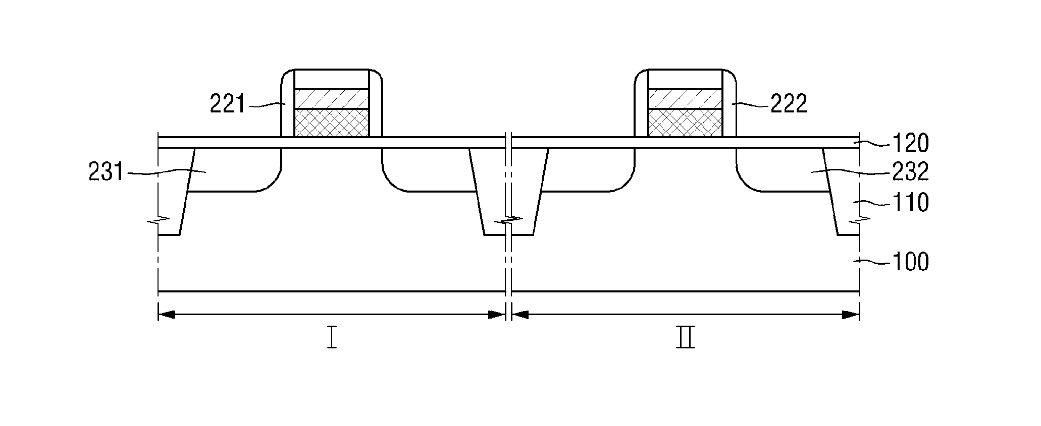
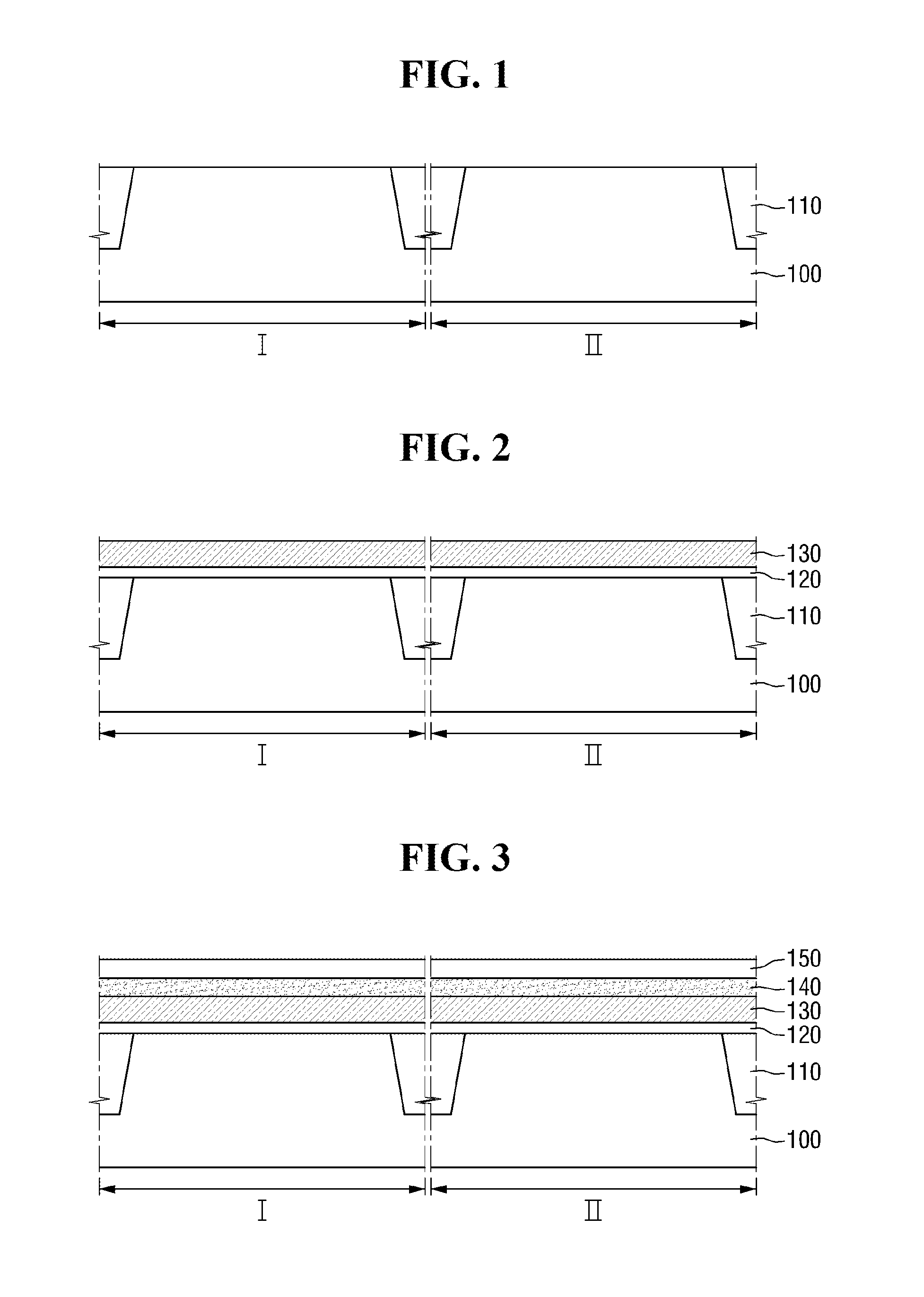
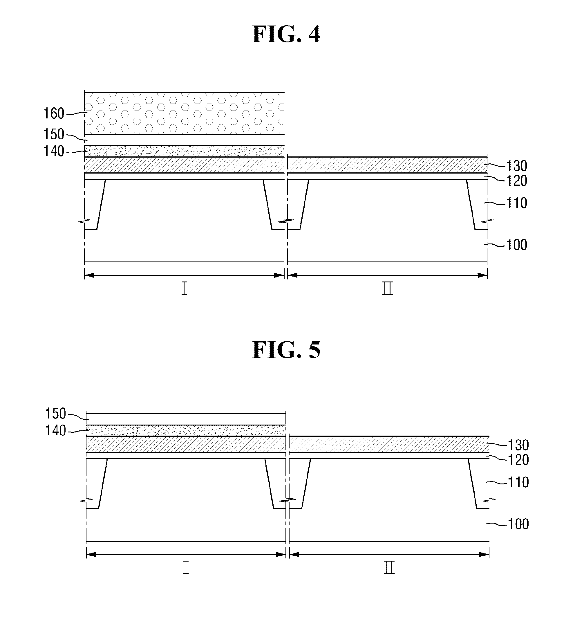
[0037]Example embodiments of the inventive concepts will now be described more fully hereinafter with reference to the accompanying drawings; however, they may be embodied in different forms and should not be construed as limited to the example embodiments set forth herein. Rather, these example embodiments are provided so that this disclosure will be thorough and complete, and will fully convey the scope of the inventive concepts to those skilled in the art.

[0038]It will also be understood that when a layer or element is referred to as being “on” another layer or substrate, it can be directly on the other layer or substrate, or intervening layers may also be present. Further, it will be understood that when a layer is referred to as being “under” another layer, it can be directly under or one or more intervening layers may also be present. In addition, it will also be understood that when a layer is referred to as being “between” two layers, it can be the only layer between the two...


PUM


Abstract

A method of manufacturing a semiconductor device having a doped layer may be provided. The method includes providing a substrate having a first region and a second region, forming a gate dielectric layer on the substrate, forming a first gate electrode layer on the gate dielectric layer, forming a first doped layer on the first gate electrode layer, forming a first capping layer on the first doped layer, forming a mask pattern on the first capping layer in the first region, the mask pattern exposing the first capping layer in the second region, removing the first capping layer and the first doped layer in the second region, removing the mask pattern, and forming a second doped layer on the first capping layer in the first region and the first gate electrode layer in the second region.

Description

CROSS-REFERENCE TO RELATED APPLICATIONS[0001]This U.S. non-provisional patent application claims priority under 35 U.S.C. §119 to Korean Patent Application No. 10-2013-0060504, filed on May 28, 2013, in the Korean Intellectual Property Office (KIPO), the contents of which are herein incorporated by reference in their entirety.BACKGROUND[0002]1. Field[0003]An aspect of the present inventive concepts herein relates to a method of manufacturing a semiconductor device having a doped layer comprising at least one of n-type and p-type impurities. The n-type or p-type impurities may be diffused into a gate electrode layer by performing an additional process, e.g., a heat treatment process.[0004]2. Description of the Related Art[0005]Responding to the growing demands for miniaturization of a semiconductor device, conductive lines, e.g., word lines or bit lines, formed in the semiconductor device have been downsized and the space between the conductive lines has been narrowed. Thus, a parasi...

Claims


Application Information

Patent Timeline
IPC IPC(8): H01L21/28
CPCH01L21/28035H01L21/28088H01L21/28079H01L21/2255H01L21/28061H01L21/823842H01L29/66575
Inventor JO, EUN-YOUNGKANG, JONG-HOONKIM, TAE-GONCHOI, HAN-MEI
Owner SAMSUNG ELECTRONICS CO LTD
Why Eureka
Try Eureka