Directed block copolymer self-assembly patterns for advanced photolithography applications

a technology of directed block and photolithography, which is applied in the direction of microstructural device manufacturing, electrical equipment, electric discharge tubes, etc., can solve the problems of poor critical dimension of strip line blocks, the lithography process is becoming more and more difficult to transfer even small features precisely and accurately without damage, and the integrated circuit has evolved into complex devices

Inactive Publication Date: 2014-12-04
APPLIED MATERIALS INC
View PDF4 Cites 137 Cited by
  • Summary
  • Abstract
  • Description
  • Claims
  • Application Information

AI Technical Summary

Benefits of technology

[0014]In yet another embodiment, a method for forming a photoresist layer by a dry development process utilizing a directed self-assembly of block copolymers process includes forming a layer of block copolymers including polystyrene and polymethylmethacrylate on a substrate wherein the polystyrene and the polymethylmethacrylate are formed in strip line forms and separately arranged in a first group and a second group of regions defined on the substrate, supplying an etching gas mixture including at least a carbon containing gas, applying a RF bias power no more than 70 Watts, and selectively etching the polymethylmethacrylate disposed on the second groups of region from the substrate in the presence of the etching gas mixture.

Problems solved by technology

Integrated circuits have evolved into complex devices that can include millions of components (e.g., transistors, capacitors and resistors) on a single chip.
Accordingly, lithography process has become more and more challenging to transfer even smaller features onto a substrate precisely and accurately without damage.
However, inaccurate control or inadequate selection of chemistries for the dry development process may result in poor critical dimension of the formed strip line block 118.
Furthermore, poor selectivity between the strip line block 118 and the strip line block 116 may also result in poor profile control and inaccurate critical dimension after etching.
These unwanted defects may result in inaccurate feature transfer to the substrate 100, thus, eventually leading to device failure and yield loss.

Method used


Image

  • Directed block copolymer self-assembly patterns for advanced photolithography applications
  • Directed block copolymer self-assembly patterns for advanced photolithography applications
  • Directed block copolymer self-assembly patterns for advanced photolithography applications

Examples


Embodiment Construction

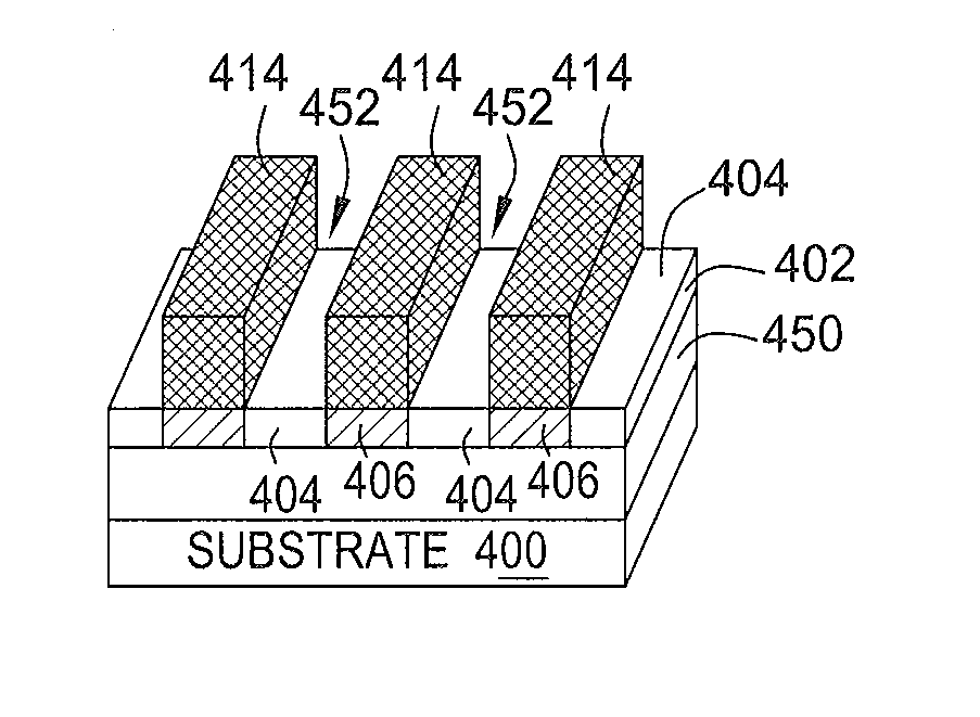
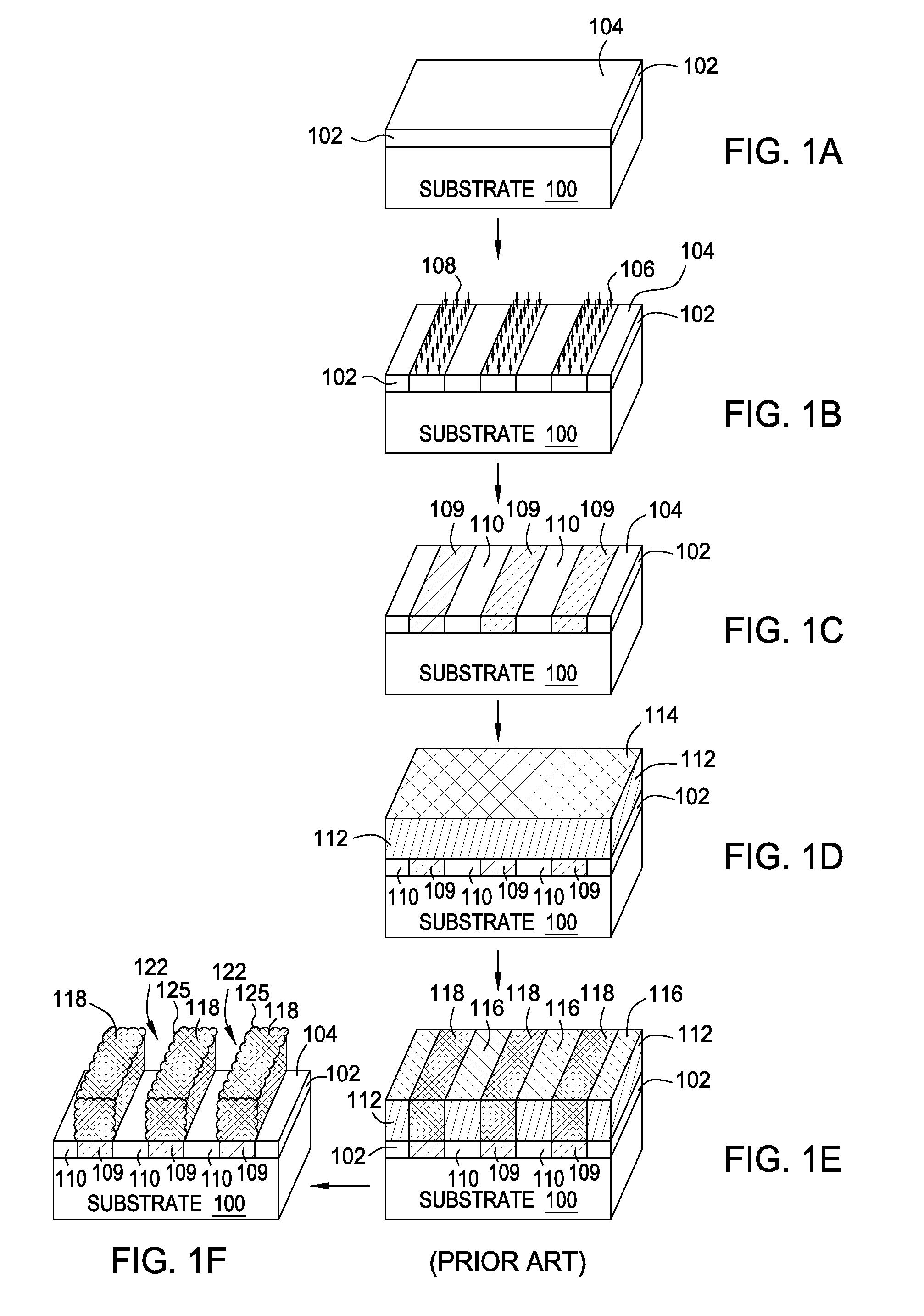
[0022]Embodiments of methods and apparatus for forming a patterned photoresist layer on a substrate to transfer features into the substrate using a directed self-assembly (DSA) of block copolymers (BCPs) process are included herein. In one embodiment, a dry development process is utilized to form a patterned photoresist layer using the directed self-assembly (DSA) of block copolymers (BCPs) process. The dry development process includes utilizing a gas mixture including at least a carbon containing gas to predominantly remove a type of polymer from the block copolymers, forming a patterned photoresist layer with desired profile on the substrate.

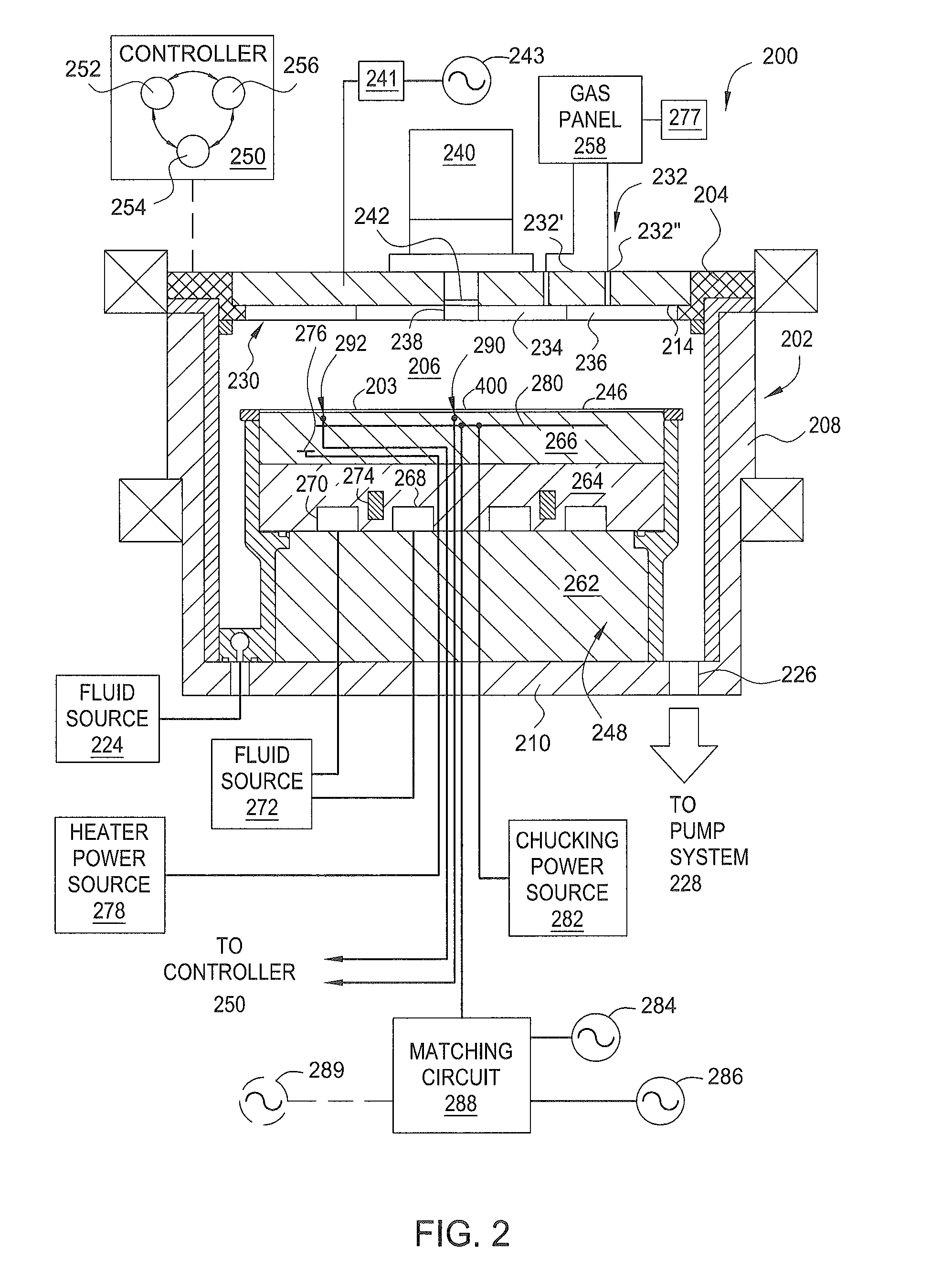
[0023]FIG. 2 is a sectional view of one embodiment of a processing chamber 200 suitable for performing an dry development process to form a patterned photoresist layer on a substrate using a directed self-assembly (DSA) of block copolymers (BCPs) process. Suitable processing chambers that may be adapted for use with the teachings disclosed her...


PUM


Abstract

Embodiments of methods and an apparatus for utilizing a directed self-assembly (DSA) process on block copolymers (BCPs) to form a defect-free photoresist layer for feature transfer onto a substrate are provided. In one embodiment, a method for performing a dry development process includes transferring a substrate having a layer of block copolymers disposed thereon into an etching processing chamber, wherein at least a first type and a second type of polymers comprising the block copolymers are aggregated into a first group of regions and a second group of regions on the substrate, supplying an etching gas mixture including at least a carbon containing gas into the etching processing chamber, and predominately etching the second type of the polymers disposed on the second groups of regions on the substrate in the presence of the etching gas mixture.

Description

CROSS-REFERENCE TO RELATED APPLICATION[0001]This application claims benefit of U.S. Provisional Application Ser. No. 61 / 829,761 filed May 31, 2013 (Attorney Docket No. APPM / 20778L), which is incorporated by reference in its entirety.BACKGROUND[0002]1. Field[0003]Embodiments generally relates to methods and apparatus for forming devices using lithography, more specifically, to methods and apparatus for forming devices using directed self-assembled (DSA) block copolymers (BCPs) as a photoresist layer in semiconductor processing technologies are provided.[0004]2. Description of the Related Art[0005]Integrated circuits have evolved into complex devices that can include millions of components (e.g., transistors, capacitors and resistors) on a single chip. The evolution of chip designs continually requires faster circuitry and greater circuit density. The demands for greater circuit density necessitate a reduction in the dimensions of the integrated circuit components.[0006]As the dimensi...

Claims


Application Information

Patent Timeline
Patent Type & Authority Applications(United States)
IPC IPC(8): H01L21/311H01L21/3065
CPCH01L21/3065H01L21/31138B81C1/00031B81C2201/0149H01J37/32935H01J37/32972H01L21/0337H01L21/31144H01L21/32139H01L21/308
Inventor LING, MANG-MANGZHU, LINAFUNG, NANCYKIM, KWANG-SOOKANG, SEAN S.NEMANI, SRINIVAS D.
Owner APPLIED MATERIALS INC
Why Eureka
Try Eureka