Curved display panel manufacturing method

a manufacturing method and technology applied in the field of curved display panel manufacturing methods, can solve the problems of high manufacturing cost of curved display panels, difficult manufacturing process of conventional flexible liquid crystal display panels, and inability to use curved displays

Inactive Publication Date: 2014-12-18
TOVIS
View PDF1 Cites 92 Cited by
  • Summary
  • Abstract
  • Description
  • Claims
  • Application Information

AI Technical Summary

Benefits of technology

[0018]According to the present invention, in a method of forming a curved display panel by paring and bending the substrates, since fixing layers are formed on edge areas near edges which are not bent in a state of being formed to the desired curved shape after paring the substr

Problems solved by technology

Such a liquid crystal display panel is generally manufactured in a flat shape, so the conventional liquid crystal display panel cannot be used as a curved display.
However, there is a problem that the manufacturing process of t

Method used


Image

  • Curved display panel manufacturing method
  • Curved display panel manufacturing method
  • Curved display panel manufacturing method

Examples


Embodiment Construction

Technical Problem

[0008]The present invention has been made in an effort to provide a curved display panel manufacturing method in which a phenomenon of separation of two substrates during paring and bending glass substrates facing one another can be prevented.

Technical Solution

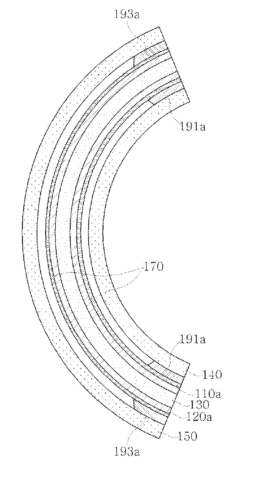
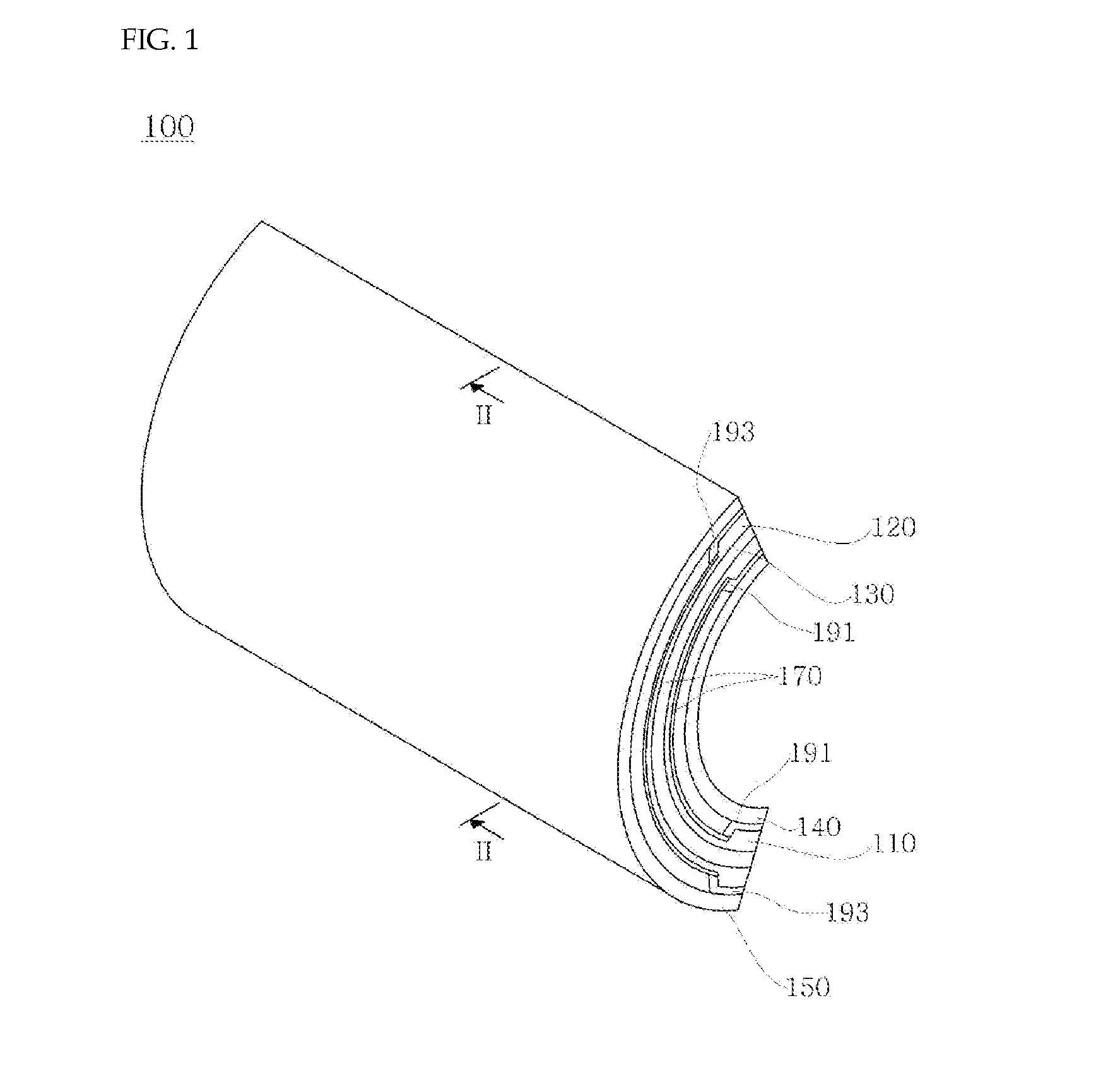
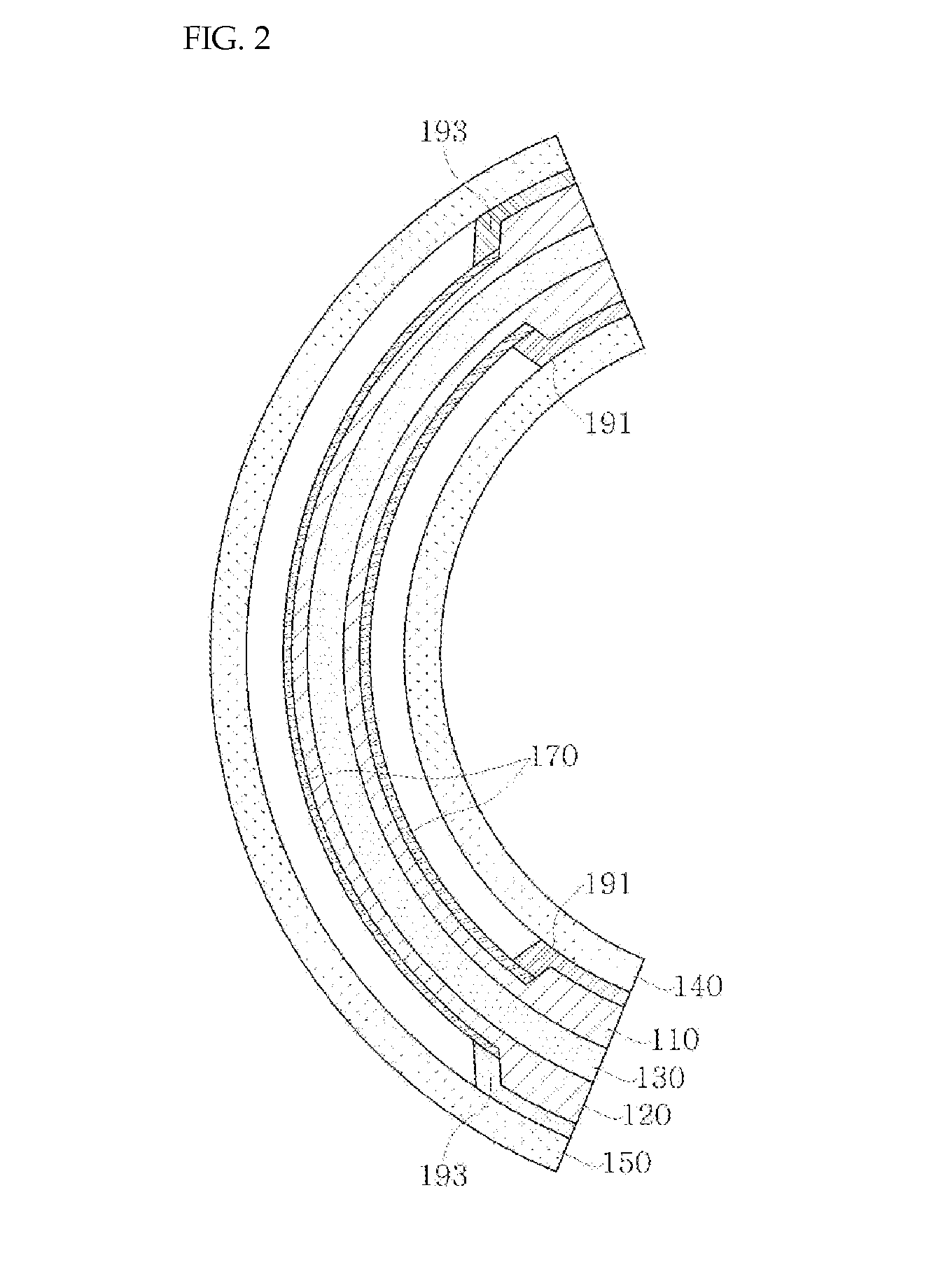
[0009]An exemplary curved display panel manufacturing method according to an embodiment of the present invention for manufacturing a curved display panel having a curved shape using a flat display panel having a first substrate and a second substrate facing one another includes: paring partially outer portions of the first substrate and the second substrate so as to reduce thicknesses thereof to predetermined thicknesses; and forming fixing layers at edge areas which are not bent in a state of being bent to the desired curved shape among the edge areas of the first substrate and the second substrate.

[0010]In the paring partially outer portions of the first substrate and the second substrate, the edge areas...


PUM


Abstract

A curved display panel manufacturing method for manufacturing a curved display panel having a curved shape using a flat display panel having a first substrate and a second substrate facing one another includes: paring partially outer portions of the first substrate and the second substrate so as to reduce thicknesses thereof to predetermined thicknesses; and forming fixing layers at edge areas which are not bent in a state of being bent to the desired curved shape among the edge areas of the first substrate and the second substrate.

Description

TECHNICAL FIELD [0001]The present invention relates to a curved display panel manufacturing method for manufacturing a display panel having a curved surface.BACKGROUND ART [0002]Various display devices have been developed and are being used. A liquid crystal display device which realizes images using liquid crystal is widely used.[0003]Generally, a liquid crystal display (LCD) includes two display panels and a liquid crystal layer disposed therebetween and having a dielectric anisotropy. An electric filed is formed in the liquid crystal layer, and a transmittance of light passing the liquid crystal layer is regulated by regulating amplitude of the electric field so as to obtain a desired image. Such a liquid crystal display is representative one of a flat panel display (FPD), and TFT-LCD which uses thin film transistor (TFT) as a switching element is widely used.[0004]A plurality of display signal lines i.e., gate lines and data lines, a plurality of thin film transistors and pixe...

Claims


Application Information

Patent Timeline
IPC IPC(8): G02F1/1333G02F1/1339B29D11/00
CPCG02F1/133305G02F1/1339B29D11/00932B29D11/0073G02F2202/28G02F1/1341G02F2201/46Y10T156/1026G02F1/133325
Inventor KIM, YONG-BEOMKIM, YANG-RAE
Owner TOVIS
Why Eureka
Try Eureka