Superlattice Structures and Infrared Detector Devices Incorporating the Same

a super-lattice structure and detector device technology, applied in the field of infrared detector devices, can solve the problems of inas/inassb sls being less practical for longer cutoff wavelengths

Active Publication Date: 2014-12-25
L3HARRIS CINCINNATI ELECTRONICS CORP
View PDF0 Cites 31 Cited by
  • Summary
  • Abstract
  • Description
  • Claims
  • Application Information

AI Technical Summary

Benefits of technology

[0009]In yet another embodiment, an infrared detector device includes a first contact layer, an absorber superlattice region, a unipolar electron or hole barrier layer, and a second contact layer. The absorber superlattice region has a period defined by an AlInAs layer, and two or more alternating InAsSb layers of an InAsSby1 layer and an InAsSby2 layer.

Problems solved by technology

This makes the InAs / InAsSb SLS less practical for longer cutoff wavelengths.

Method used


Image

  • Superlattice Structures and Infrared Detector Devices Incorporating the Same
  • Superlattice Structures and Infrared Detector Devices Incorporating the Same
  • Superlattice Structures and Infrared Detector Devices Incorporating the Same

Examples


Embodiment Construction

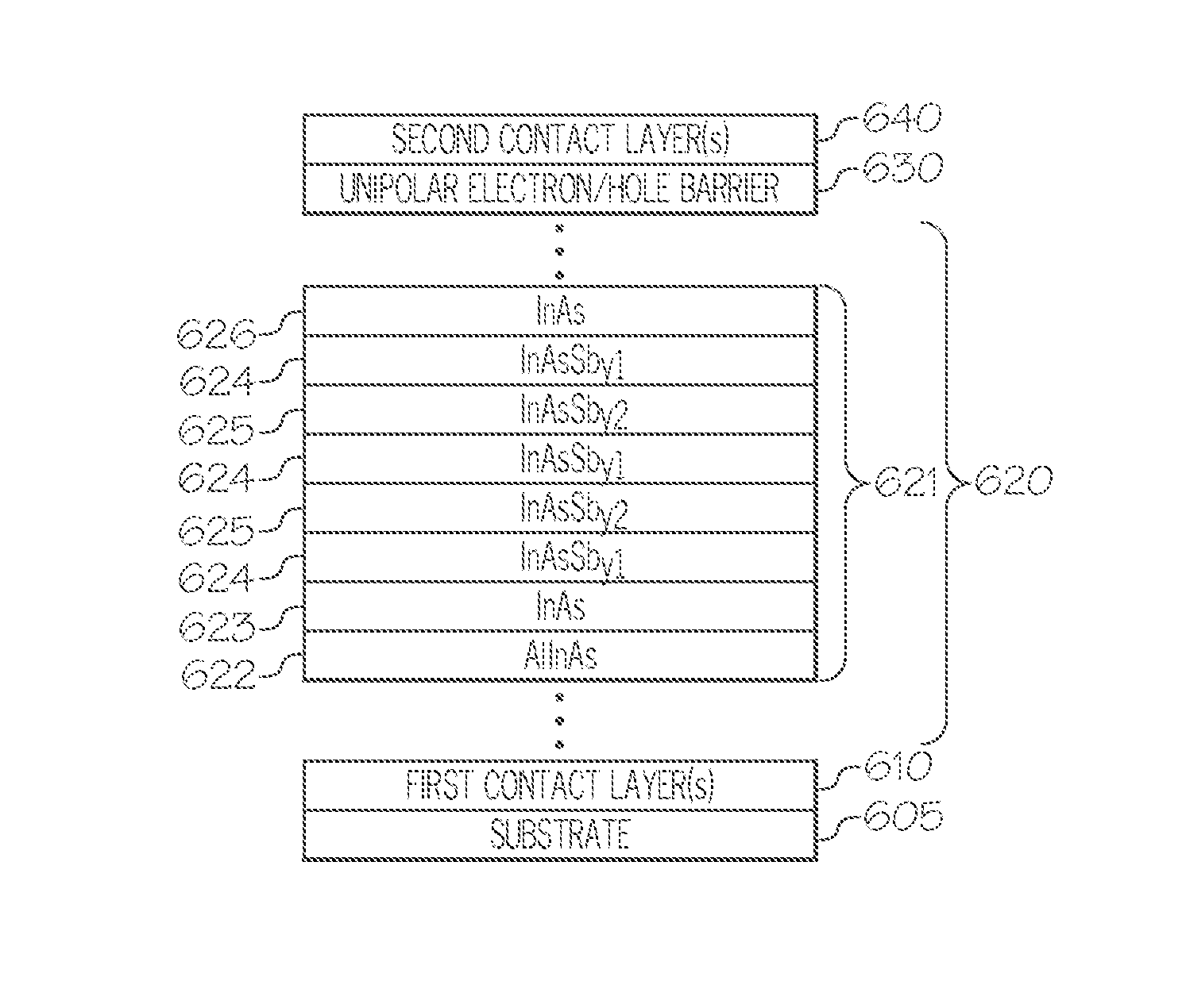
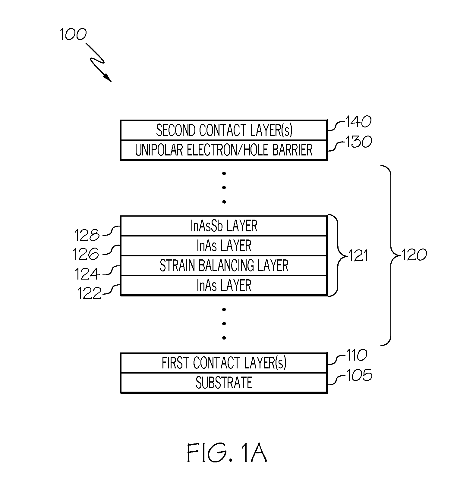
[0024]Embodiments of the present disclosure are generally directed to infrared detector devices (e.g., barrier infrared detector devices (“BIRD”)) regardless of wavelength regime, e.g., short wavelength infrared (“SWIR”), mid wavelength infrared (“MWIR”), long wavelength infrared (“LWIR”), very long wavelength infrared (“VLWIR”), etc. to increase quantum efficiency (“QE”) and reduce the hole effective mass of superlattice structure (“SLS”) infrared detector devices. As an example and not a limitation, the InAs / InGaAs / InAs / InAsSb superlattice structures and other superlattice structures described herein may be provided in the absorber region of the diode barrier infrared detector devices (“DBIRD”) described in U.S. patent application Ser. No. 14 / 271,908 filed on May 7, 2014 entitled “DIODE BARRIER INFRARED DETECTOR DEVICES AND SUPERLATTICE BARRIER STRUCTURES,” which is hereby incorporated by reference in its entirety.

[0025]In embodiments of the present disclosure, a strain-balancing ...


PUM


Abstract

Embodiments of strain-balanced superlattice infrared detector devices and their fabrication are disclosed. In one embodiment, an infrared detector device includes a first contact layer, and absorber superlattice region, a wider gap unipolar barrier region, and a second contact layer. The absorber superlattice region has a period defined by a first InAs layer, strain-balancing structure, a second InAs layer, and an InAsSb layer. The strain-balancing structure comprises an arbitrary alloy layer sequence containing at least one constituent element of aluminum or phosphor, e.g., InGaAs, AlInAs InAsP. In another embodiment, the absorber superlattice region has a period defined by a first InAs layer, first strain-balancing structure, a second InAs layer, a first GaSb layer, a second strain-balancing structure, and a second GaSb layer. The first strain-balancing structure includes at least one constituent element of aluminum or phosphor, e.g., InGaAs, AlInAs InAsP. The second strain-balancing structure includes GaInSb and GaSb.

Description

CROSS-REFERENCE TO RELATED APPLICATIONS[0001]This application claims the benefit of U.S. Provisional Application No. 61 / 839,158 filed on Jun. 25, 2013.BACKGROUND[0002]1. Field[0003]The present specification generally relates to infrared detector devices and, more particularly, to infrared detector devices having a strain-balanced superlattice structure.[0004]2. Technical Background[0005]The nBn device structure generally includes an n-type absorber layer, a barrier layer to block majority carriers, and an n-type contact layer. The introduction of InAs / InAsSb superlattice structure (“SLS”) material has enabled the nBn type device structure and has boosted the operating temperature of mid-wave infrared (“MWIR”) focal plane arrays (“FPAs”) using III-V materials. For the InAs / InAsSb superlattice structure (“SLS”) material, band gap tuning is achieved by tuning the Sb composition and the InAsSb layer thickness, while InAs layer is provided as a strain-balancing layer mostly to balance ou...

Claims


Application Information

Patent Timeline
Patent Type & Authority Applications(United States)
IPC IPC(8): H01L31/0352H01L31/0304
CPCH01L31/03046H01L31/035236H01L31/101Y02E10/544
Inventor WEI, YAJUN
Owner L3HARRIS CINCINNATI ELECTRONICS CORP
Why Eureka
Try Eureka