Semiconductor integrated circuit device

a technology of integrated circuits and semiconductors, applied in the direction of semiconductor devices, electrical equipment, transistors, etc., can solve problems such as high side drive circuit malfunctions, and achieve the effects of reducing intervals, and reducing (practically eliminating) hole implantation

Active Publication Date: 2015-01-15
FUJI ELECTRIC CO LTD
View PDF2 Cites 22 Cited by
  • Summary
  • Abstract
  • Description
  • Claims
  • Application Information

AI Technical Summary

Benefits of technology

[0040]Also, the semiconductor integrated circuit device according to the heretofore described aspect of the invention is characterized by further including a resistance layer provided across a dielectric on the surface of the first second conductivity type region, wherein the drain of the insulated gate field effect transistor is electrically connected to the resistance layer via a wiring layer disposed on the first conductivity type semiconductor substrate.
[0041]According to the invention, by the cavity being formed between the first conductivity type low potential region and first conductivity type isolation region, and the first conductivity type region being provided above the cavity to a depth reaching the cavity, it is possible to extract holes flowing from the first conductivity type low potential region to the first conductivity type isolation region when negative surge occurs in the connection point of the first and second elements, and thus possible to reduce (practically eliminate) hole implantation.
[0042]Also, according to the invention, the first conductivity type region is not deeper than a depth reaching the cavity, because of which it is possible to prevent the first conductivity type region from punching through to the first conductivity type semiconductor substrate due to a transient rise in the potential of the connection point of the first element and second element. Also, according to the invention, it is possible to reduce (practically eliminate) hole implantation by the hole pick-up first conductivity type region being provided to a depth reaching the cavity, because of which it is possible to reduce the interval between the first conductivity type low potential region and the circuit portion.
[0043]According to the semiconductor integrated circuit device according to the invention, there is an advantage in that it is possible to avoid an occurrence of malfunction or destruction. Also, according to the semiconductor integrated circuit device according to the invention, there is an advantage in that it is possible to reduce chip size.

Problems solved by technology

Because of this, there is a problem in that the high side drive circuit malfunctions.

Method used


Image

  • Semiconductor integrated circuit device
  • Semiconductor integrated circuit device
  • Semiconductor integrated circuit device

Examples


embodiment 1

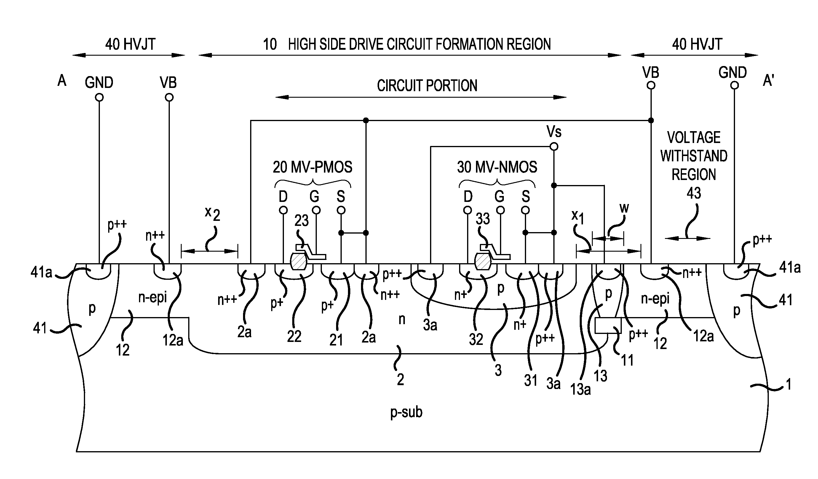
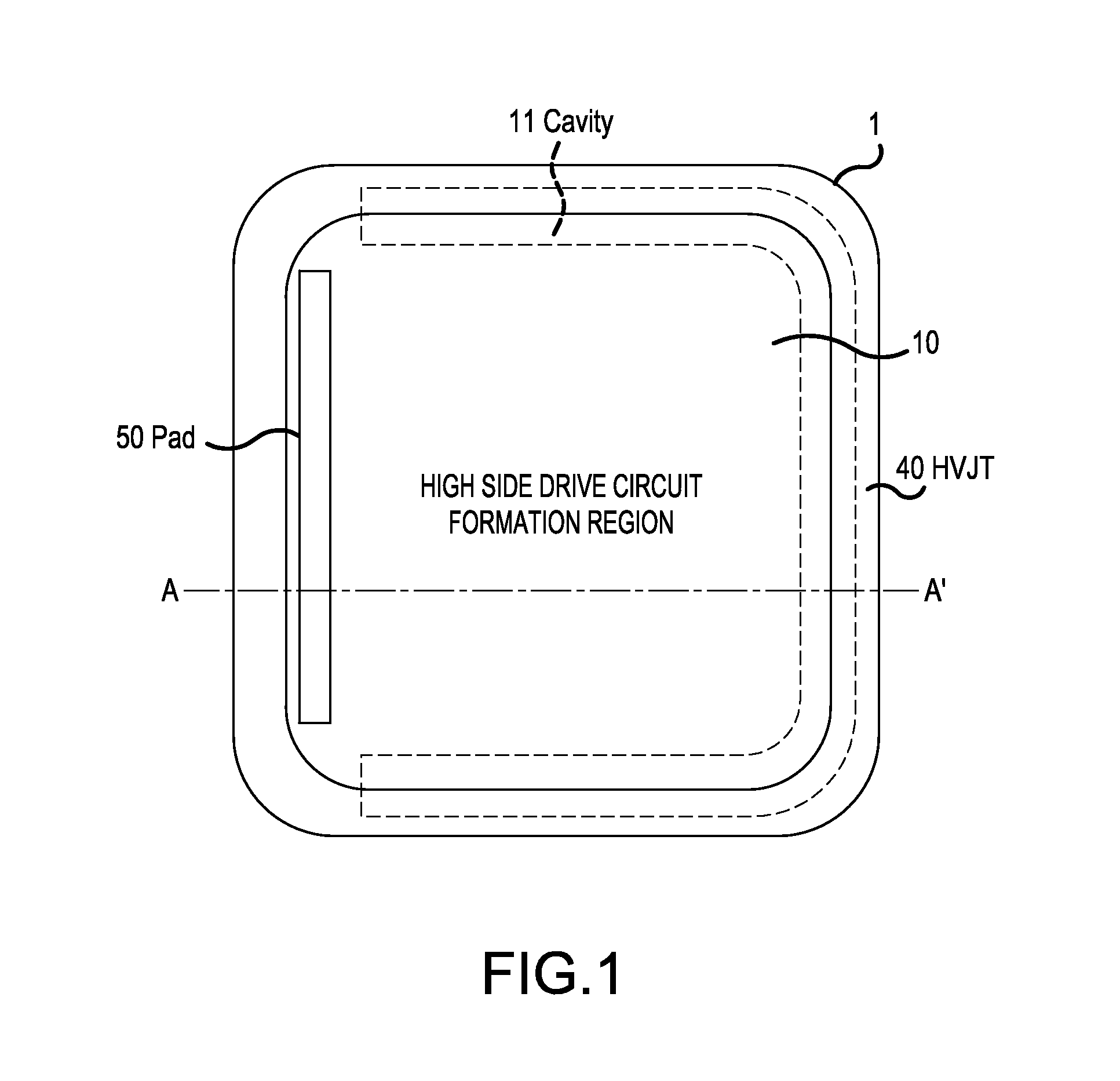
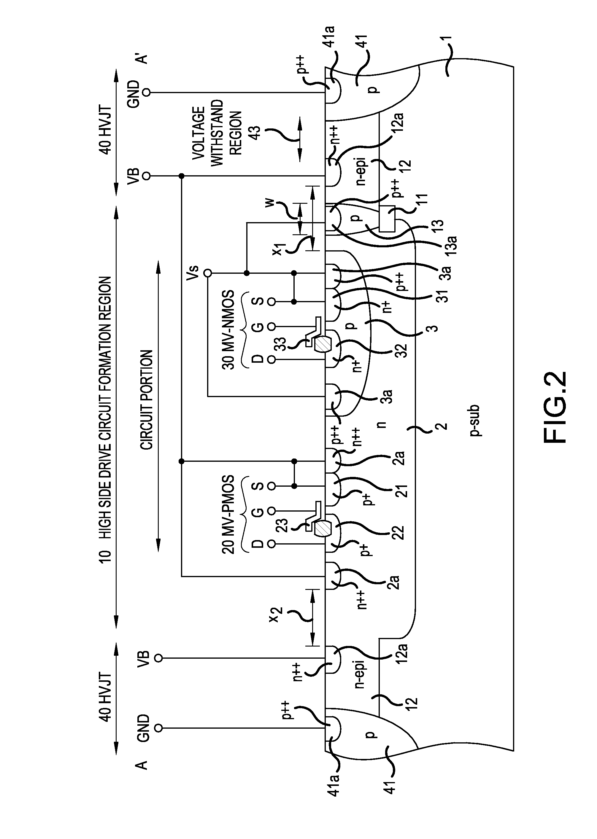
[0061]A description will be given of a semiconductor integrated circuit device according to Embodiment 1, using as an example a high side drive circuit that drives an upper arm output element of a drive circuit wherein upper and lower arm driver functions are mounted on one silicon chip. FIG. 1 is a plan view showing a planar structure of the semiconductor integrated circuit device according to Embodiment 1. FIG. 2 is a sectional view showing a sectional structure along a section line A-A′ of FIG. 1. As the configuration of a drive circuit including the semiconductor integrated circuit device according to Embodiment 1 is the same as, for example, the configuration (one phase) of a drive circuit 111 shown in FIG. 9, a description will be omitted.

[0062]The semiconductor integrated circuit device according to Embodiment 1 is, for example, a high side drive circuit of the drive circuit 111, which drives an upper arm output element (first MOSFET 101: first element) of a power module (out...

embodiment 2

[0101]Next, a description will be given of a semiconductor integrated circuit device according to Embodiment 2. FIG. 15 is a plan view showing a planar structure of the semiconductor integrated circuit device according to Embodiment 2. FIG. 16 is a sectional view showing a sectional structure along a section line B-B′ of FIG. 15. The semiconductor integrated circuit device according to Embodiment 2 differs from the semiconductor integrated circuit device according to Embodiment 1 in that, in a self-shielding type high side drive circuit wherein a level shifter is integrated with the HVJT 40, no n++ type high concentration region (corresponding to reference sign 12a of FIG. 14) for applying (picking-up) the high side power supply potential VB to the HVJT 40 is provided in the n-type epitaxial region (n− type region) 12.

[0102]In Embodiment 2, it is possible to reduce the chip size by an amount commensurate with no n++ type high concentration region being provided in the n-type epitaxi...


PUM


Abstract

An MV-PMOS and MV-NMOS configuring a high side drive circuit are formed in an n-type isolation region formed on a p-type semiconductor substrate. The MV-NMOS is connected to a p-type isolation region of an intermediate potential in the interior of the n-type isolation region. An n-type epitaxial region is provided in a surface layer of the p-type semiconductor substrate on the outer side of the n-type isolation region, and a p-type GND region of a ground potential (GND) is provided on the outer side of the n-type epitaxial region. A cavity is provided between the p-type semiconductor substrate and n-type epitaxial region between the high side drive circuit and p-type GND region, and a p-type diffusion region is provided penetrating the n-type epitaxial region and reaching the cavity. The intermediate potential is applied to the p-type isolation region.

Description

CROSS-REFERENCE TO RELATED APPLICATIONS[0001]This application is a continuation of International Application No. PCT / JP2013 / 071079, filed on Aug. 2, 2013, which is based on and claims priority to Japanese Patent Application No. JP 2012-202126, filed on Sep. 13, 2012. The disclosure of the Japanese priority application and the PCT application in their entirety, including the drawings, claims, and the specification thereof, are incorporated herein by reference.BACKGROUND OF THE INVENTION[0002]1. Field of the Invention[0003]The present invention relates to a semiconductor integrated circuit device.[0004]2. Related Art[0005]Besides motor control inverters, power devices are widely utilized in a large number of fields, such as a power supply application of a PDP (plasma display panel), liquid crystal panel, or the like, with a large capacitive load, or an inverter application for household appliances such as air conditioners or lighting. In recent years, owing to advances in LSI technolo...

Claims


Application Information

Patent Timeline
Patent Type & Authority Applications(United States)
IPC IPC(8): H01L27/092H01L29/10H01L29/06
CPCH01L29/0649H01L29/1083H01L27/0921H01L21/761H01L21/823871H01L21/823878H01L27/092H01L27/1207
Inventor IMAI, TOMOHIROYAMAJI, MASAHARU
Owner FUJI ELECTRIC CO LTD
Why Eureka
Try Eureka