
Integration of the silicon impatt diode in an analog technology

a technology of impatt diodes and silicon, applied in the direction of diodes, semiconductor devices, electrical apparatus, etc., can solve the problems of reducing the contribution of skin effect to series resistance, phase delay between ac current and ac voltage, and the mesa shape impatt diodes in fig. 1 becoming difficult to adopt at terahertz

Active Publication Date: 2015-01-22
TEXAS INSTR INC
View PDF4 Cites 3 Cited by
  • Summary
  • Abstract
  • Description
  • Claims
  • Application Information

AI Technical Summary

Benefits of technology

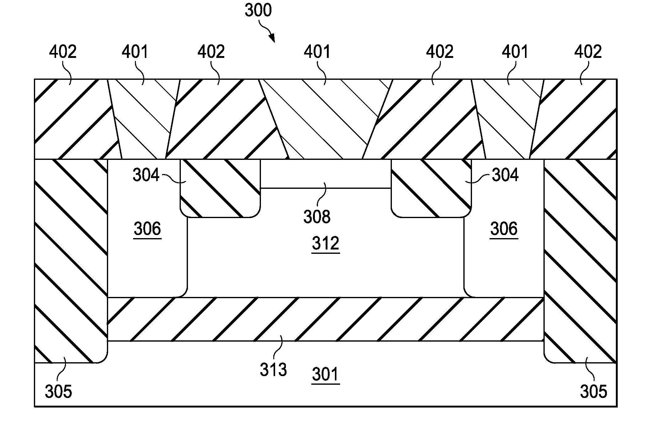
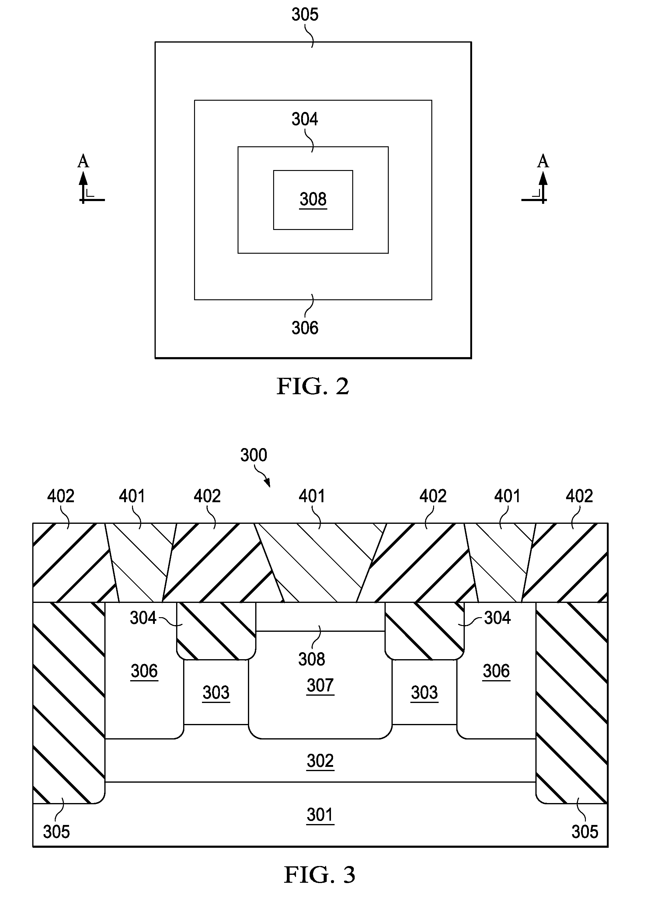
This patent describes a vertical IMPATT diode that can be fabricated using a standard planar analog process. The diode includes a substrate, an n-type buried layer, an un-doped layer, a deep trench, a shallow trench layer, a layer of material, and ohmic contacts. The method for making the diode involves depositing layers and forming trenches. The technical benefits of this invention include providing a compact and efficient vertical diode structure for use in analog circuits, reducing circuit size and complexity, and improving performance and reliability.

Problems solved by technology

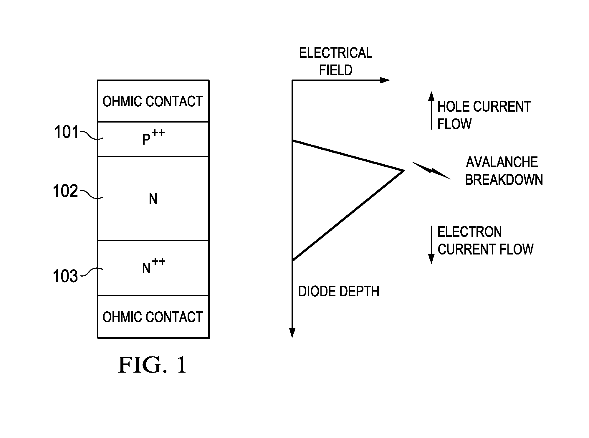
All three carriers can then participate in further avalanching collisions, leading to a sudden multiplication of carriers in the space-charge region when the maximum filed becomes large enough to cause avalanche,
Under alternating current (AC) condition, the diode AC current, coming from the moving electrons within the device, can lag behind the AC voltage applied on the diode, resulting in phase delay between AC current and AC voltage.
Minimizing substrate resistivity also reduces the skin effect contribution to the series resistance.
The discrete mesa shape IMPATT diode in FIG. 1 becomes difficult to adopt at Terahertz regime.

Method used


Image

  • Integration of the silicon impatt diode in an analog technology
  • Integration of the silicon impatt diode in an analog technology
  • Integration of the silicon impatt diode in an analog technology

Examples


Embodiment Construction

[0023]The present invention is described with reference to the attached figures. The figures are not drawn to scale and they are provided merely to illustrate the invention. Several aspects of the invention are described below with reference to example applications for illustration. It should be understood that numerous specific details, relationships, and methods are set forth to provide an understanding of the invention. One skilled in the relevant art, however, will readily recognize that the invention can be practiced without one or more of the specific details or with other methods. In other instances, well-known structures or operations are not shown in detail to avoid obscuring the invention. The present invention is not limited by the illustrated ordering of acts or events, as some acts may occur in different orders and / or concurrently with other acts or events. Furthermore, not all illustrated acts or events are required to implement a methodology in accordance with the pre...


PUM


Abstract

A method to integrate a vertical IMPATT diode in a planar process.

Description

CROSS-REFERENCE TO RELATED APPLICATIONS[0001]This application claims the benefit of priority under U.S.C. §119(e) of U.S. Provisional Application 61 / 847,742 (Texas Instruments docket number TI-72793PS, filed Jul. 18, 2013).FIELD OF THE INVENTION[0002]This invention relates to the field of semiconductor devices. More particularly, this invention relates to integration of the IMPact Avalanche Transit-Time (IMPATT) diode into the analog technology.BACKGROUND OF THE INVENTION[0003]The IMPATT diode is a 2-terminal device with typical applications in the area of radio frequency (RF) power generation and amplification. Compared to a 3-terminal device approach, the IMPATT diode can be fabricated to have very small resistive loss and parasitic capacitance. Therefore, the IMPATT diode can generate high RF power at high frequency, making it especially useful for the Terahertz (>300 GHz) applications.[0004]A conventional n-type IMPATT diode, as shown in FIG. 1 consists of three distinct regi...

Claims


Application Information

Patent Timeline
IPC IPC(8): H01L29/66H01L29/864
CPCH01L29/66159H01L29/864H01L29/165H01L27/0635H01L29/0649H01L29/161
Inventor BI, XIAOCHUANKRAKOWSKI, TRACEYWEISER, DOUG
Owner TEXAS INSTR INC
Learn More