A kind of lateral structure impatt diode and preparation method thereof

A lateral structure, diode technology, applied in diodes, semiconductor/solid-state device manufacturing, semiconductor devices, etc., can solve the problems that restrict the performance of traditional vertical structure IMPATT, difficult metal-P-type GaN barrier height, and difficult to form high-quality P-type ohmic contact and other problems, to achieve the effect of enhancing low field mobility, significant negative differential mobility effect, and reducing device size

Active Publication Date: 2021-04-30
NORTHWEST UNIV
View PDF5 Cites 0 Cited by
  • Summary
  • Abstract
  • Description
  • Claims
  • Application Information

AI Technical Summary

Problems solved by technology

However, the forbidden band width of GaN material is too large, which is 3.4eV. The typical value of the metal work function available in the current process is generally around 4 to 5eV, and it is difficult to form a lower metal-P-type GaN barrier height difference.
Second, the free hole concentration in P-type doped GaN is too low, and it is difficult to obtain a high free hole concentration even with a high doping level
To sum up, in the traditional GaN-based IMPATT with vertical structure, it is difficult to form high-quality P-type ohmic contacts due to the immature manufacturing technology of P-type GaN, which limits the concentration of charge packets generated by impact ionization, and seriously Restricts the working performance of the traditional vertical structure IMPATT

Method used


Image

  • A kind of lateral structure impatt diode and preparation method thereof
  • A kind of lateral structure impatt diode and preparation method thereof
  • A kind of lateral structure impatt diode and preparation method thereof

Examples


Embodiment Construction

[0041] The present invention will be described in further detail below in conjunction with specific examples, but not as a limitation of the present invention.

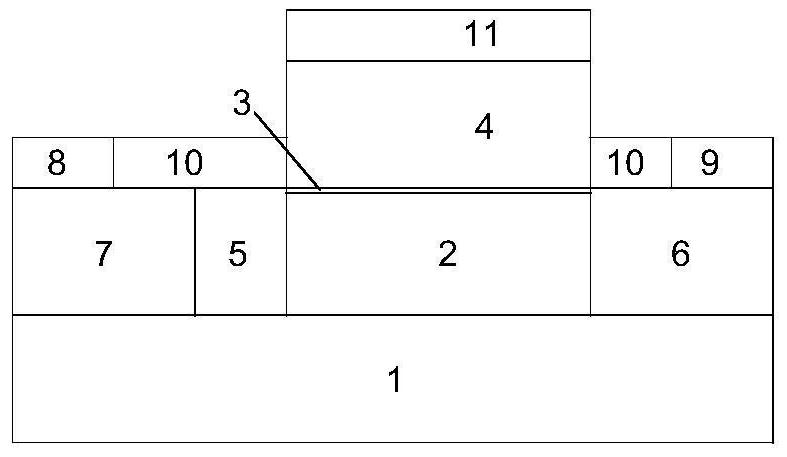
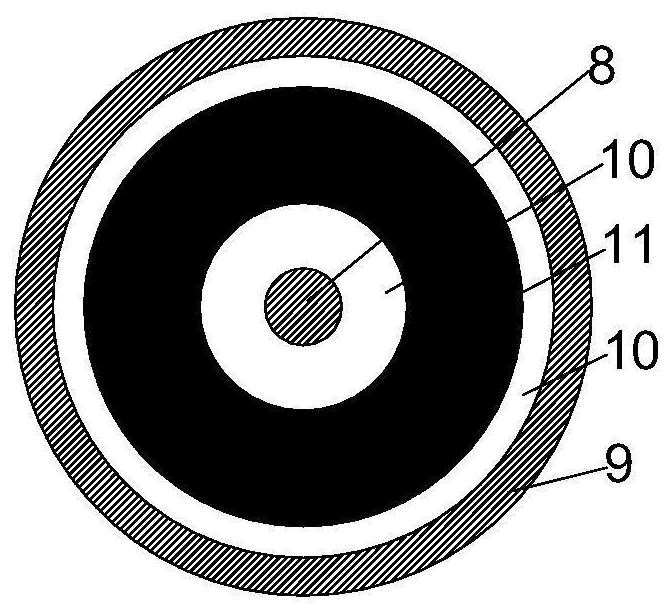
[0042] refer to figure 2 , the lateral structure IMPATT diode of the present invention comprises a substrate layer 1, an epitaxial layer 2, a drift layer 3, an n-AlGaN barrier layer 4, an n+-GaN barrier layer 5, a right ohmic contact layer 6, a left ohmic contact layer 7, a left Ohmic contact electrode 8 , right ohmic contact electrode 9 , passivation layer 10 , Schottky contact electrode 11 .

[0043] The epitaxial layer 2 is located on the upper layer of the substrate layer 1; the drift layer 3 is a two-dimensional electron gas thin layer formed on the top of the epitaxial layer 2 when electricity is applied; the n-AlGaN barrier layer 4 is located on the upper layer of the drift layer 3; n+-GaN The barrier layer 5 is located on the upper layer of the substrate layer 1 and on the left side of the epitaxial layer 2;...


PUM

PropertyMeasurementUnit
thicknessaaaaaaaaaa
thicknessaaaaaaaaaa
diameteraaaaaaaaaa

Abstract

The invention discloses a lateral structure IMPATT diode and a preparation method thereof. The IMPATT diode comprises: a substrate layer, an epitaxial layer, a drift layer, an n-AlGaN barrier layer, an n+-GaN barrier layer, a left ohmic contact layer, and a right ohmic contact layer , left ohmic contact electrode, right ohmic contact electrode, passivation layer, Schottky contact electrode, lateral structure IMPATT diode The current direction is along the lateral direction of the epitaxial layer when the diode is energized, and the drift layer is a two-dimensional electron gas thin layer formed on the top of the epitaxial layer , the transition process is limited to the drift layer instead of taking place in the bulk material. The IMPATT proposed by the present invention utilizes the lateral structure. Under the same material, the oscillation frequency, lateral circuit compatibility, and frequency flexibility of the traditional vertical structure IMPATT are improved. .

Description

technical field [0001] The invention belongs to the technical field of semiconductors, and relates to a lateral structure IMPATT diode and a preparation method thereof. Background technique [0002] Avalanche diode (IMPATT) is a semiconductor device that uses impact ionization in semiconductors to generate charge packets, and the charge packets pass through to generate negative resistance at a certain frequency. Because avalanche will produce avalanche delay, carriers drifting inside the device through a finite time will produce transit time delay. The superposition of these two delays will cause the establishment of avalanche current to lag behind the terminal voltage, thus generating negative resistance. When the sum of these two delays falls within the range of 1 / 4 cycle to 3 / 4 cycle (90° to 270° phase difference), the dynamic resistance of the diode is negative at this time. As one of the most efficient and powerful microwave solid-state sources, IMPATT diodes have rece...

Claims


Application Information

Patent Timeline
Patent Type & Authority Patents(China)
IPC IPC(8): H01L29/864H01L29/06H01L21/329
CPCH01L29/0603H01L29/66219H01L29/864
Inventor 戴扬卢昭阳雷晓艺张云尧廖晨光贠江妮闫军锋王雪文赵武张志勇陈晓江
Owner NORTHWEST UNIV
Why Eureka
Try Eureka