

High-frequency IMPATT diode mesa die structure and preparation method thereof
A diode and mesa technology, used in semiconductor/solid-state device manufacturing, electrical components, circuits, etc., can solve the problems of poor reliability, reduce device negative resistance, and reduce RF power efficiency, and increase the heat sink area. , Improve the output power and reduce the effect of additional resistance
- Summary
- Abstract
- Description
- Claims
- Application Information
AI Technical Summary
Problems solved by technology
Method used
Image

Examples
Embodiment Construction
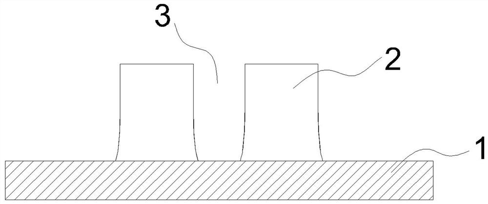
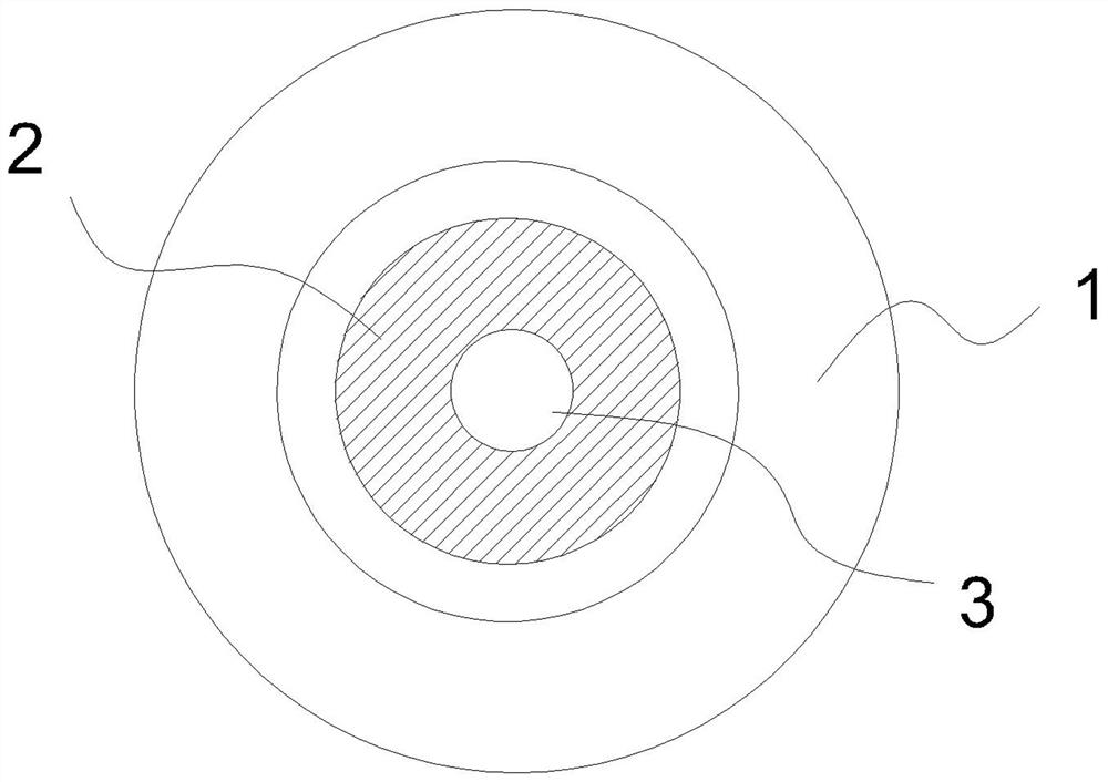
[0025] combine figure 1 and figure 2 As shown, the present invention provides a high-frequency IMPATT diode mesa tube core structure, including a p+ conductive substrate 1, a mesa tube core pn junction 2 is provided on the top surface of the p+ conductive substrate, and a vertical The through hole 3 makes the mesa tube core form a circular frustum shape; the diameter of the lower part of the through hole 3 is tapered from top to bottom.
[0026] The present invention also provides a kind of preparation method of high-frequency IMPATT diode mesa die structure, comprises the following steps:
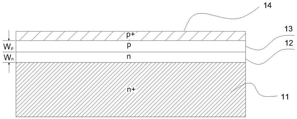
[0027] S1, combine image 3 As shown, an n-type epitaxial layer 12, a p-type epitaxial layer 13 and a p+ epitaxial layer 14 are sequentially grown on an n+ silicon wafer 11;
[0028] The thickness Wn of n-type epitaxial layer 12 is given by the formula (1) decide,
[0029] The thickness Wp of the p-type epitaxial layer 13 is given by the formula (2) decide,
[0030] In formulas...
PUM
 Abstract
Description
Claims
Application Information