HEMT epitaxial device based on third-generation semiconductor GaN material and growth method thereof

A semiconductor and epitaxy technology, applied in semiconductor devices, semiconductor/solid-state device manufacturing, electrical components, etc., can solve the problem of unstable gate voltage pinch-off current characteristics, decreased channel 2DEG mobility, and weakened gate-to-current Control and other issues to achieve the effect of improving I-V characteristics, improving the overall crystal quality, and reducing additional resistance

Pending Publication Date: 2021-11-16
王晓波
View PDF0 Cites 0 Cited by
  • Summary
  • Abstract
  • Description
  • Claims
  • Application Information

AI Technical Summary

Problems solved by technology

Its chip has the characteristics of high reverse blocking voltage, low forward conduction resistance, and high operating frequency, so it can meet the system's requirements for semiconductor devices with higher power, higher frequency, and smaller volume. With the advancement of technology, HEMT The performance and reliability requirements of the chip are getting higher and higher, but there are still many problems due to the epitaxial growth method and structure of the third-generation semiconductor material;
[0003] One: increase the output current and increase the output power. With the expansion of the application direction, the output current and power of HMET need to be further improved. At present, the current output increase of HMET is to increase the concentration of 2DEG (two-dimensional electron gas), and the traditional double-isolated Mass junction structure dual-channel or multi-channel 2DEG, AlGaN / GaN / AlGaN / GaN, InAlN / GaN / InAlN / GaN, AlN / GaN / AlN / GaN or other heterojunctions are arranged alternately and sequentially. The strip materials have their own 2DEG, and the built-in electric field direction is consistent, but the two heterojunctions in the middle also have 2DEG, and the built-in electric field direction is opposite to that on both sides. Although two-channel or multi-channel 2DEG can increase the current output, However, the reverse electric field at the middle heterojunction of the traditional two-channel structure will make the gate voltage control unstable and the pinch-off current characteristics will be poor. The middle reverse electric field will weaken the control of the gate current, which is not conducive to the overall performance. .
[0004] Second: The high GaN background electron concentration leads to leakage channels and parasitic currents. Metal elements such as Fe, Cr, and Mg are introduced into GaN epitaxial growth to form deep energy level defects or provide holes to compensate for the remaining carriers to obtain high Although the GaN` layer with resistance value can improve the high resistance state of GaN, the doping of the epitaxial layer is not easy to control, which will lead to material deterioration. At the same time, the introduction of impurities will reduce the mobility of the channel 2DEG, which will affect the device characteristics. New methods are urgently needed to improve
[0005] Third: The most important problem of HMET epitaxy is that defects will appear during the epitaxial growth process, especially at the contact interface of the material, which will cause many lattice adaptation problems, and cracks and position defects will appear in the single-layer thick material during the thickness growth process. Wrong, especially with high Al content

Method used


Image

  • HEMT epitaxial device based on third-generation semiconductor GaN material and growth method thereof
  • HEMT epitaxial device based on third-generation semiconductor GaN material and growth method thereof
  • HEMT epitaxial device based on third-generation semiconductor GaN material and growth method thereof

Examples


Embodiment 1

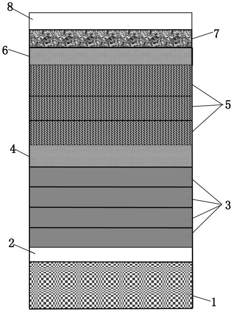
[0074] A HEMT epitaxial device based on the third-generation semiconductor GaN material, using metal organic compound chemical vapor deposition (MOCVD) epitaxial growth technology, using trimethylgallium (TMGa), trimethylindium (TMIn), trimethylaluminum ( TMAl), ammonia (NH 3 ), silane (SiH 4 ) respectively provide the gallium source, indium source, aluminum source, nitrogen source, and silicon source required for growth, with nitrogen and hydrogen as carrier gases;

[0075] (1) Clean the substrate with dilute hydrochloric acid and isopropanol, then rinse with water and dry it, put it into MOCVD equipment and bake at 1200°C for 10 minutes;

[0076] (2) Cool down the equipment to 500°C, pressure 150torr, feed trimethylgallium and ammonia to grow a layer of 10nm GaN, then raise the temperature to 1020°C, pressure 250torr, grow 100nm GaN;

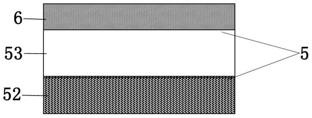
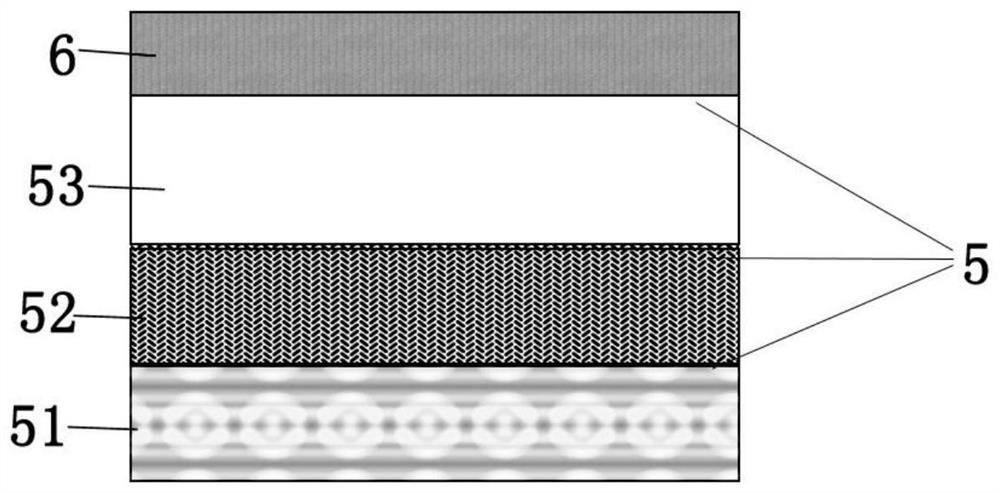
[0077] (3) At 1040°C, with an air pressure of 300torr, inject trimethylaluminum, trimethylgallium and ammonia to grow a layer of 1nm Al 0....

Embodiment 2

[0088] A HEMT epitaxial device based on the third-generation semiconductor GaN material, using metal organic compound chemical vapor deposition (MOCVD) epitaxial growth technology, using trimethylgallium (TMGa), trimethylindium (TMIn), trimethylaluminum ( TMAl), ammonia (NH 3 ), silane (SiH 4 ) respectively provide the gallium source, indium source, aluminum source, nitrogen source, and silicon source required for growth, with nitrogen and hydrogen as carrier gases;

[0089] (1) Clean the substrate with dilute hydrochloric acid and isopropanol, then rinse with water and dry it, put it into MOCVD equipment and bake at 1200°C for 10 minutes;

[0090] (2) Cool down the equipment to 500°C, air pressure 150torr, feed trimethylgallium and ammonia gas to grow a layer of 20nm GaN, then raise the temperature to 1020°C, air pressure 250torr, grow 200nm GaN;

[0091] (3) At 1040°C, with an air pressure of 300torr, inject trimethylaluminum, trimethylgallium and ammonia to grow a layer o...

Embodiment 3

[0102] A HEMT epitaxial device based on the third-generation semiconductor GaN material, using metal organic compound chemical vapor deposition (MOCVD) epitaxial growth technology, using trimethylgallium (TMGa), trimethylindium (TMIn), trimethylaluminum ( TMAl), ammonia (NH 3 ), silane (SiH 4 ) respectively provide the gallium source, indium source, aluminum source, nitrogen source, and silicon source required for growth, with nitrogen and hydrogen as carrier gases;

[0103] (1) Clean the substrate with dilute hydrochloric acid and isopropanol, then rinse with water and dry it, put it into MOCVD equipment and bake at 1200°C for 10 minutes;

[0104] (2) Cool down the equipment to 500°C, air pressure 150torr, feed trimethylgallium and ammonia gas to grow a layer of 12nm GaN, then raise the temperature to 1020°C, air pressure 250torr, grow 150nm GaN;

[0105] (3) At 1040°C, with an air pressure of 300torr, inject trimethylaluminum, trimethylgallium and ammonia to grow a layer o...


PUM

PropertyMeasurementUnit
thicknessaaaaaaaaaa
thicknessaaaaaaaaaa
thicknessaaaaaaaaaa

Abstract

The invention discloses an HEMT epitaxial device based on a third-generation semiconductor GaN material. Heteroepitaxial growth is carried out on a substrate by adopting an MOCVD technology; the HEMT epitaxial device comprises a substrate, a first GaN layer, a depletion high-resistance region, an Al Ga<1-z>N layer, a 2DEG channel, an AlN layer, an AlGaN layer and a second GaN layer which are sequentially stacked from bottom to top. A superlattice structure formed by gradually changing and combining components such as GaN/Al<x>Ga<1-x>N-SL is adopted, and the stress of material growth can be reduced; meanwhile, due to the fact that the forbidden band width of the material is gradually increased upwards from the substrate, background electrons move to a low-energy region, a built-in electric field pointing to the substrate is formed, a local region depletion layer is generated, the free electron concentration is greatly reduced, a higher-resistance region is formed, and current collapse and electric leakage channels are reduced.

Description

technical field [0001] The invention relates to the technical field of novel semiconductors, in particular to a HEMT epitaxial device based on the third-generation semiconductor GaN material and a growth method thereof. Background technique [0002] The third-generation wide-bandgap semiconductors represented by gallium nitride (GaN) and aluminum nitride (AlN) have wide bandgap constants, higher electron mobility, strong radiation resistance, and good breakdown electric field strength. , high temperature resistance and other characteristics, are being widely concerned by people, the heterojunction high electron mobility transistor (HEMT) based on the compound AlGaN / GaN, (or heterojunction field effect transistor HFET, modulation doped field effect transistor MODFET , hereinafter collectively referred to as HEMT chips) have been widely used in the semiconductor field. Its chip has the characteristics of high reverse blocking voltage, low forward conduction resistance, and hi...

Claims


Application Information

Patent Timeline
Patent Type & Authority Applications(China)
IPC IPC(8): H01L29/778H01L21/335H01L29/15H01L29/20
CPCH01L29/778H01L29/66462H01L29/151H01L29/2003
Inventor 王晓波
Owner 王晓波
Why Eureka
Try Eureka