A kind of graphene enhanced thin film transistor and preparation method thereof

A technology of thin-film transistors and graphene films, applied in the field of sensors, can solve problems such as impact, and achieve the effects of reducing additional resistance, shortening distance, and improving electrical injection efficiency

Active Publication Date: 2022-08-02
HUIZHOU UNIV
View PDF7 Cites 0 Cited by
  • Summary
  • Abstract
  • Description
  • Claims
  • Application Information

AI Technical Summary

Problems solved by technology

However, due to the special mobility anisotropy of organic semiconductor materials, the device with the upper electrode structure is affected by the thickness of the material.
The thicker the semiconductor layer material, the greater the additional resistance added to the device. In order to reduce the problem caused by the anisotropy of the mobility, the influence of the thickness of the accessory is reduced by reducing the thickness of the material, but the reduction of the material thickness is also Increased device instability

Method used


Image

  • A kind of graphene enhanced thin film transistor and preparation method thereof
  • A kind of graphene enhanced thin film transistor and preparation method thereof
  • A kind of graphene enhanced thin film transistor and preparation method thereof

Examples


Embodiment Construction

[0028] The present invention will be described in detail below with reference to the accompanying drawings and examples, and the examples are only preferred embodiments of the present invention, and are not intended to limit the present invention.

[0029] A preparation method of a graphene-enhanced thin film transistor, comprising the following steps:

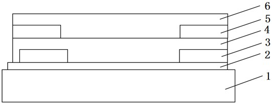
[0030] S1. Graphene films are prepared on the substrate, and 1-2 layers of graphene films can be grown on the substrate in situ, or the graphene films grown on other substrates can be transferred to the target substrate by means of transfer;

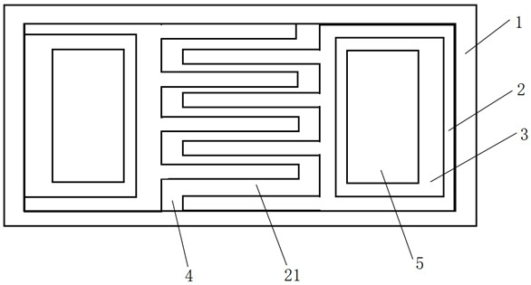
[0031] S2. Graphene film patterning, the graphene film patterning can be vapor-deposited by means of leakage plate vapor deposition sacrificial layer, or photolithography is obtained after spin-coating photoresist on the surface of the graphene film, or nano-pressure Printing, screen printing and other graphic methods;

[0032] S3. The bottom electrode is prepared on the surface of the ...


PUM

PropertyMeasurementUnit
thicknessaaaaaaaaaa
thicknessaaaaaaaaaa
thicknessaaaaaaaaaa

Abstract

The invention belongs to the technical field of sensors. A method for preparing a graphene-enhanced thin film transistor, comprising the following steps: preparing a graphene film on a substrate; patterning the graphene film; preparing a bottom electrode on the surface of the patterned graphene film; The organic semiconductor material is grown on the surface to form a functional layer; the top electrode is prepared by electron beam evaporation on the surface of the functional layer; the PMMA film is spin-coated on the surface of the top electrode and the functional layer to form a protective layer. The preparation method of the invention has good controllability, and by presetting the graphene film on the substrate, the ordered orientation of the organic semiconductor material can be induced, the film-forming quality of the organic semiconductor material is improved, and the overall performance of the device is effectively improved . The prepared thin film transistor has a double-layer electrode structure, high electron injection efficiency, and can improve the saturated output current and overall performance of the transistor.

Description

technical field [0001] The invention belongs to the technical field of sensors, and in particular relates to a graphene-enhanced thin film transistor and a preparation method thereof. Background technique [0002] Organic thin film transistors are semiconductor devices that use organic materials instead of traditional inorganic materials. Compared with traditional inorganic semiconductor materials, organic materials have more advantages. For example, the active layer can be obtained by spin coating, inkjet printing of polymers and organic small molecule materials at room temperature, and the production temperature is low to achieve low cost. In addition, organic materials have the advantages of easy availability of raw materials, large area, flexibility, etc., so the future development prospects are broad. However, the carrier mobility of organic thin film transistors still has a certain gap with traditional thin film transistor materials, and improving the mobility of orga...

Claims


Application Information

Patent Timeline
Patent Type & Authority Patents(China)
IPC IPC(8): H01L51/05H01L51/10H01L51/40
CPCH10K10/482H10K10/82
Inventor 刘舸李元元
Owner HUIZHOU UNIV
Why Eureka
Try Eureka