Image forming apparatus

a technology of image forming apparatus and forming apparatus, which is applied in the direction of electrographic process apparatus, instruments, corona discharge, etc., can solve the problems of image deletion increased risk of occurrence of charging failure, etc., and achieves the effect of increasing the amount of discharge current and favorable charging

Active Publication Date: 2015-01-22
KONICA MINOLTA INC
View PDF4 Cites 0 Cited by
  • Summary
  • Abstract
  • Description
  • Claims
  • Application Information

AI Technical Summary

Benefits of technology

[0011]The present invention is made in view of the above-described problems, and aims to provide an image forming apparatus that is capable of realizing favorable charging by increasing the amount of discharge current without increasing the peak-to-peak voltage Vpp.
[0012]To achieve the aim, one aspect of the present invention provides an image forming apparatus for forming an image from an electrostatic latent image generated by exposing an electrically charged photoreceptor to light, comprising: a contact charging unit that is in contact with a photoreceptor and electrically charges the photoreceptor by causing electric discharge; a bias applying unit that applies an alternating current bias to the contact charging unit; and a superposing unit that superposes a direct current bias onto the alternating current bias, the direct current bias having a same polarity as a charge polarity of the photoreceptor, wherein the alternating current bias has a same waveform as a rectangular wave bias during a period in which an absolute value of the alternating current bias is smaller than an absolute value of a predetermined boundary voltage, and the absolute value of the alternating current bias increases at a slower rate than an absolute value of the rectangular wave bias during a period in which the absolute value of the alternating current bias is equal to or greater than an absolute value of a discharge start voltage, the discharge start voltage being a voltage at which the electric discharge occurs between the contact charging unit and the photoreceptor and having a same polarity as the charge polarity of the photoreceptor, and the absolute value of the predetermined boundary voltage being no greater than the absolute value of the discharge start voltage, and a discharge time provided by the alternating current bias, for which the absolute value of the alternating current bias is equal to or greater than the absolute value of the discharge start voltage, is longer than the discharge time provided by a sinusoidal wave bias having a same frequency and a same amplitude as the alternating current bias, and is no longer than the discharge time provided by a rectangular wave bias having the same frequency and the same amplitude as the alternating current bias.

Problems solved by technology

However, if the discharge current is increased in amount under a high-humidity environment, image deletion, which is caused by adhesion of the product of the discharge, will become more likely to occur.
Under a low-temperature and low-humidity environment, the charging device increases in electrical resistance for example, and there is a risk of the occurrence of a charging failure.
Therefore, in either of the conventional technologies, an increase in parts cost and manufacturing cost is inevitable.
Furthermore, since it is necessary to improve the voltage endurance in order to increase the peak-to-peak voltage Vpp, an increase in cost and power consumption of the power supply device for example is also inevitable.
Moreover, the increase in peak-to-peak voltage Vpp also causes problems such as short life as well as the image deletion resulting from the increase in the product of the discharge as described above, because the photoreceptor wears out quickly due to the high voltage.

Method used


Image

  • Image forming apparatus
  • Image forming apparatus
  • Image forming apparatus

Examples


Embodiment Construction

[0027]The following describes an image forming apparatus pertaining to an embodiment of the present invention, with reference to the drawings.

[0028][1] Structure of Image Forming Apparatus

[0029]First of all, the structure of an image forming apparatus pertaining to the present embodiment is described.

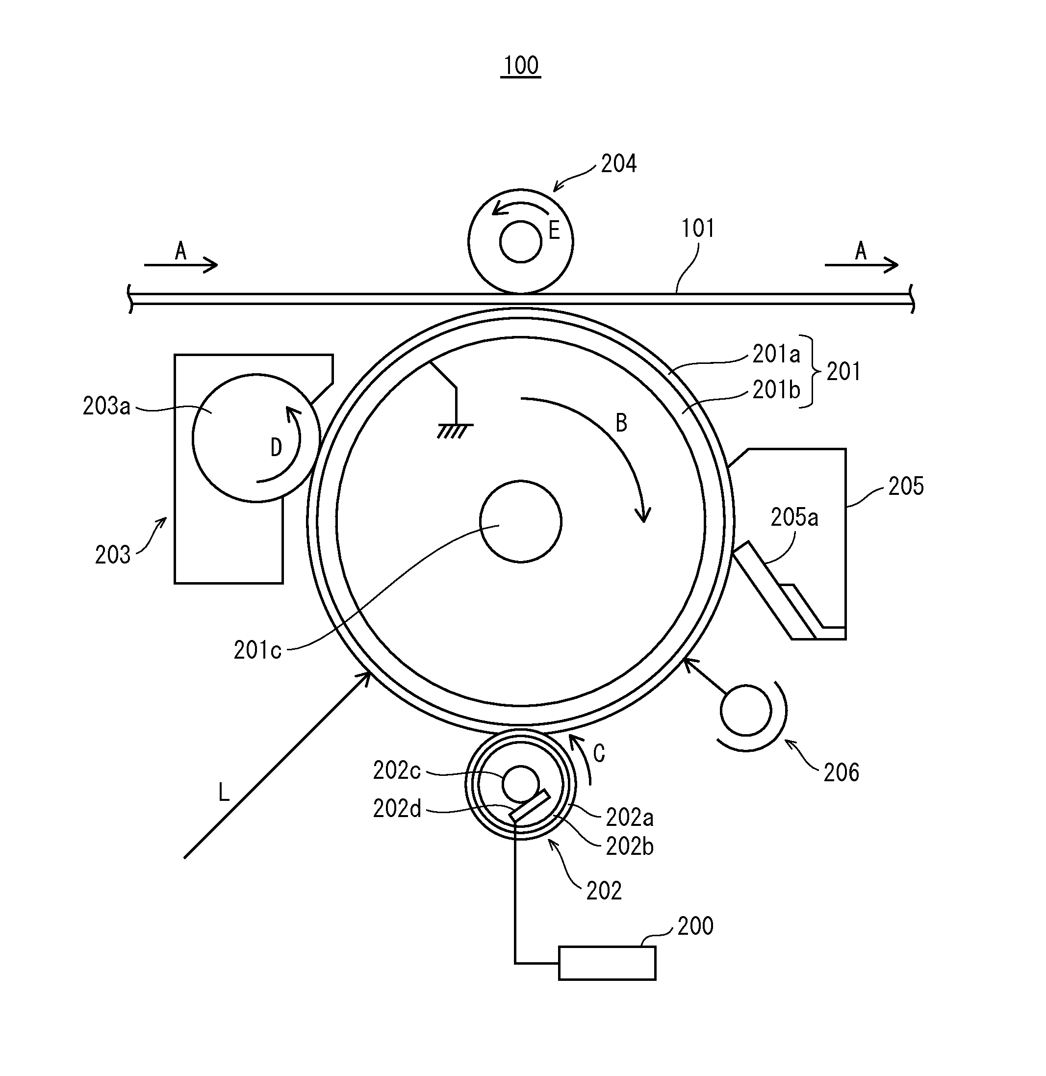
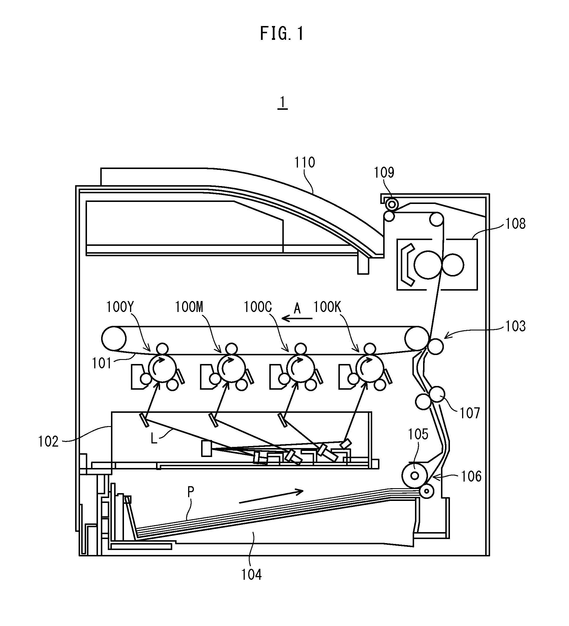
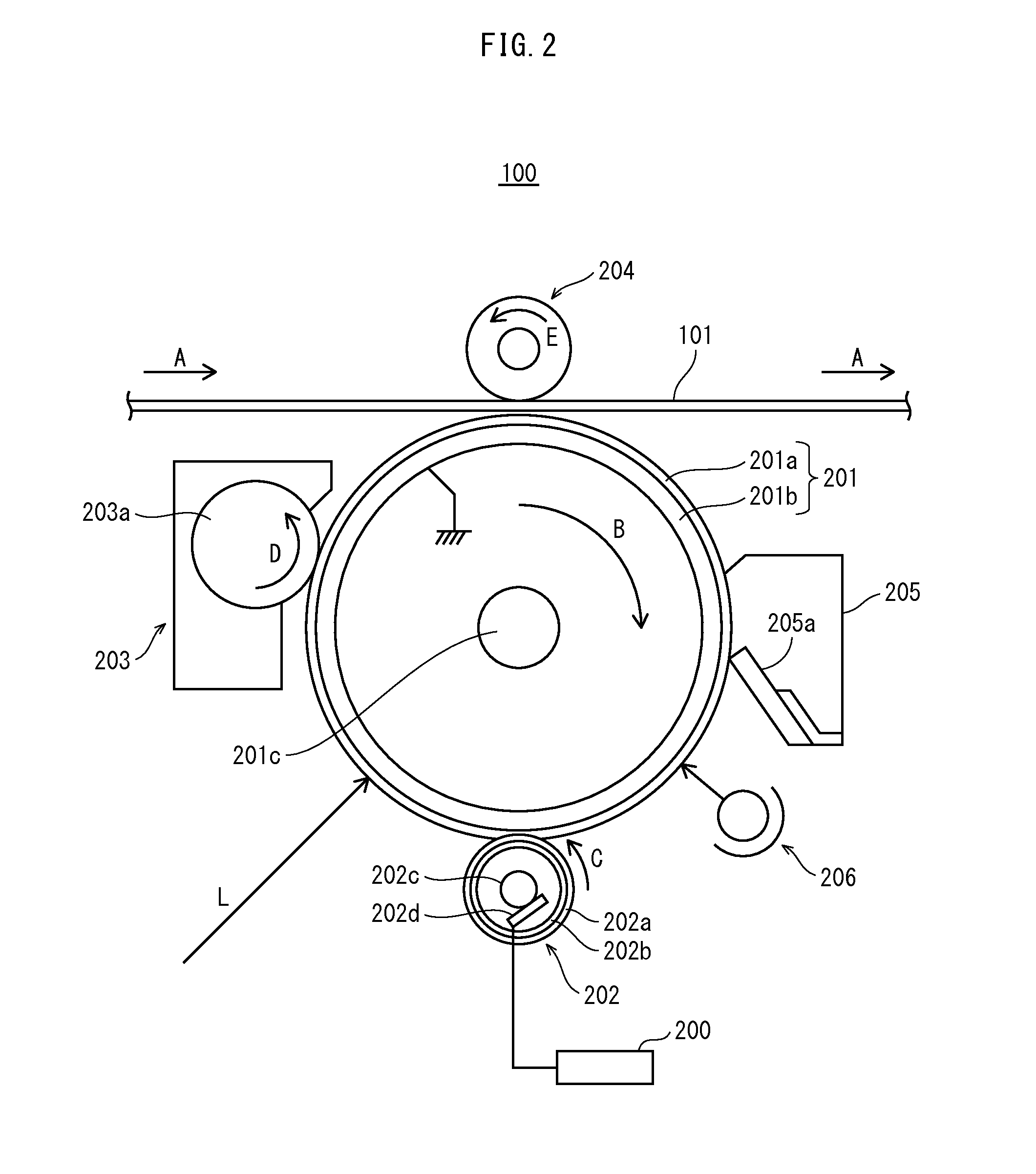
[0030]As shown in FIG. 1, an image forming apparatus 1 pertaining to the present embodiment is a tandem color printer, and image creating units 100Y through 100K are arranged along an intermediate transfer belt 101. The image creating units 100Y through 100K each receive image exposure light (L) from an exposure device 102 and respectively form toner images of the colors yellow (Y), magenta (M), cyan(C) and black (K). Then, the image creating units 100Y through 100K statically transfer the toner images on the intermediate transfer belt 101 so that the images overlap each other on the intermediate transfer belt 101 (i.e. primary transfer). Thus a color toner image is formed. Alternativel...


PUM


Abstract

An image forming apparatus including: a contact charging unit that is in contact with a photoreceptor and electrically charges the photoreceptor by causing electric discharge; a bias applying unit that applies an AC bias to the contact charging unit; and a superposing unit that superposes a DC bias onto the AC bias, the DC bias having a same polarity as a charge polarity of the photoreceptor. The AC bias has a same waveform as a rectangular wave bias during a period in which an absolute value of the AC bias is smaller than an absolute value of a predetermined boundary voltage, and the absolute value of the AC bias increases at a slower rate than an absolute value of the rectangular wave bias during a period in which the absolute value of the AC bias is equal to or greater than an absolute value of a discharge start voltage.

Description

CROSS-REFERENCE TO RELATED APPLICATIONS[0001]This application is based on application No. 2013-148634 filed in Japan, the contents of which are hereby incorporated by reference.BACKGROUND OF THE INVENTION[0002](1) Field of the Invention[0003]The present invention relates to electrophotographic image forming apparatuses and in particular to technology of charging a photoreceptor in a preferable manner by securing a sufficient amount of discharge current without applying high voltage.[0004](2) Related Art[0005]In an electrophotographic image forming apparatus, it is necessary to uniformly charging the surface of a photoreceptor before forming an electrostatic latent image on the surface of the photoreceptor. Methods of charging can be classified roughly into non-contact charging methods and contact charging methods. Examples of the contact charging methods include a roller charging method and a brush charging method. The roller charging method is a method of charging the surface of th...

Claims


Application Information

Patent Timeline
Patent Type & Authority Applications(United States)
IPC IPC(8): G03G15/02
CPCG03G15/0266G03G15/0216
Inventor OSADA, MORIO
Owner KONICA MINOLTA INC
Why Eureka
Try Eureka