Optical device and manufacturing method thereof

Inactive Publication Date: 2015-01-29
ELECTRONICS & TELECOMM RES INST
View PDF6 Cites 9 Cited by
  • Summary
  • Abstract
  • Description
  • Claims
  • Application Information

AI Technical Summary

Benefits of technology

[0006]The present invention provides an optical device an optical dev

Problems solved by technology

The indirect bandgap material has a limitation in that it may not be used as a light source because light emission efficiency of the material is low.
Generally, the flip chip bonding method needs an alignment error smaller than about 1 μm

Method used


Image

  • Optical device and manufacturing method thereof
  • Optical device and manufacturing method thereof
  • Optical device and manufacturing method thereof

Examples


Example

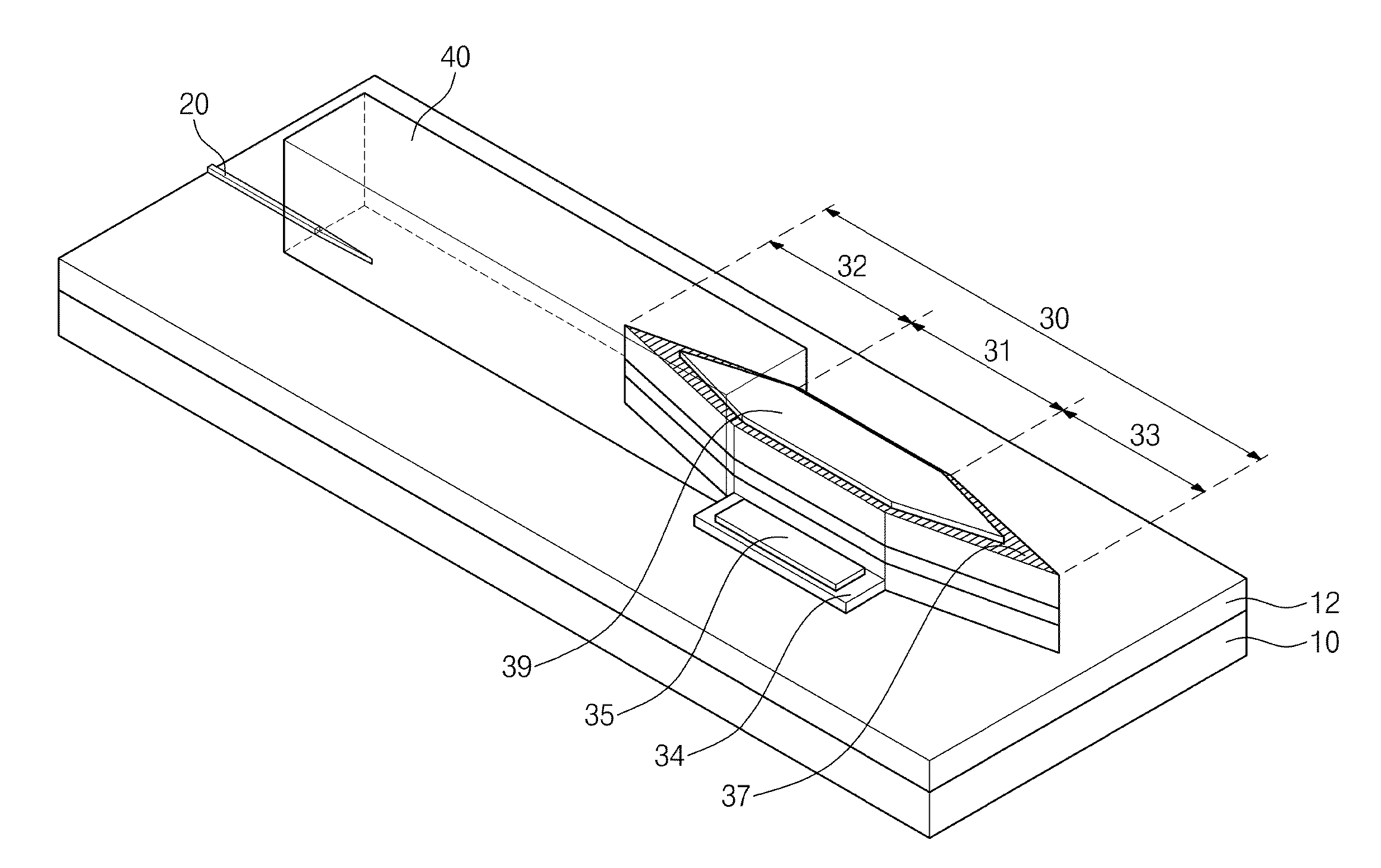
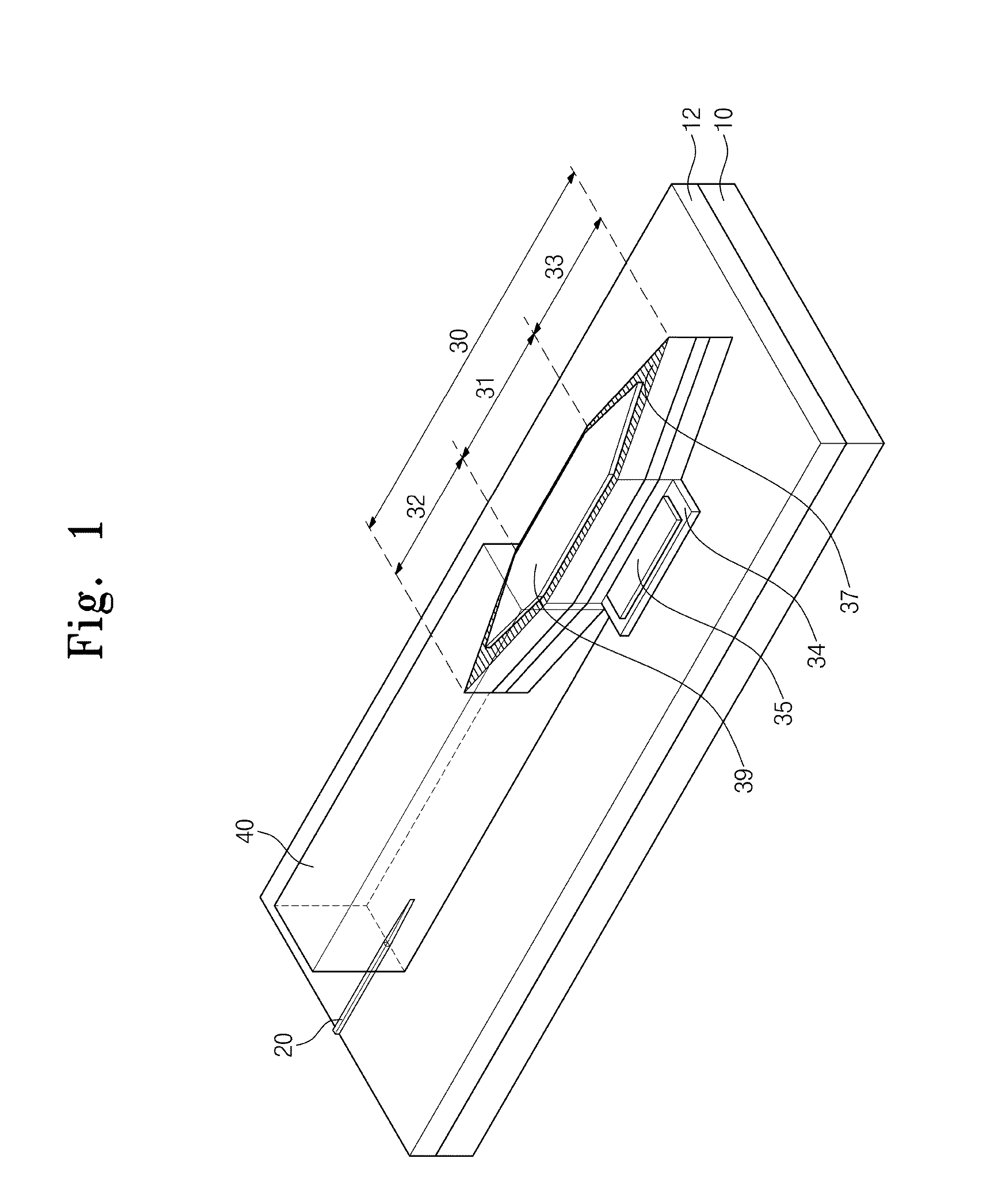
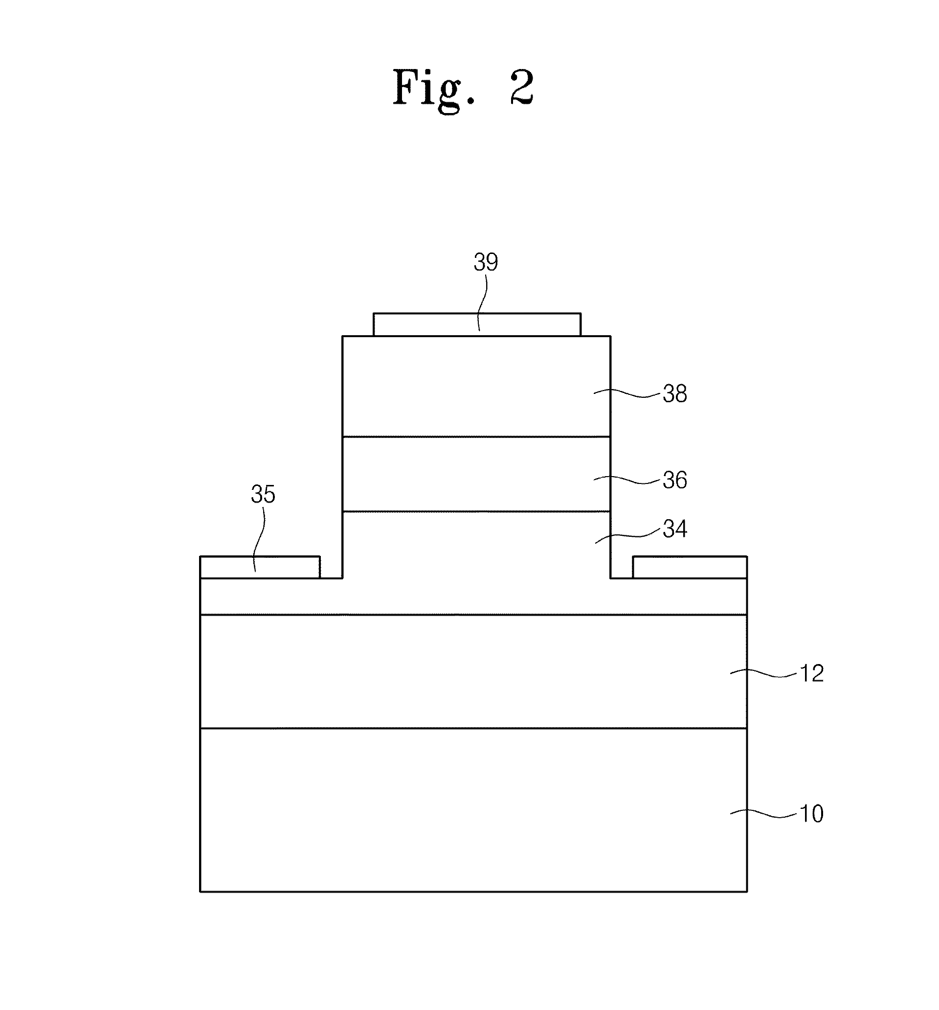
[0049]Thus, the optical device according to a first embodiment of the inventive concept may enhance productivity.

Example

[0050]FIG. 5 is a perspective view of an optical device according to a second embodiment of the inventive concept.

[0051]Referring to FIG. 5, the optical device according to the second embodiment of the inventive concept may include a second optical waveguide 22 and a second coupled waveguide 42 disposed on the other side of the laser 30 facing the first optical waveguide 20 and the first coupled waveguide 40,. The first coupled waveguide 40 and the second coupled waveguide 42 may have second Bragg diffraction gratings 80. The second Bragg diffraction grating 80 may include pin holes or polymer. The laser 30 may generate a laser light having a wavelength corresponding to the period of the second Bragg diffraction gratings 80. As compared to the first embodiment, the second embodiment further includes the second optical waveguide 22, the second coupled waveguide 42, and the second Bragg diffraction gratings 80.

Example

[0052]FIG. 6 is a perspective view of an optical device according to a third embodiment of the inventive concept.

[0053]Referring to FIG. 6, the optical device according to the third embodiment of the inventive concept may include third Bragg diffraction gratings 90 that are formed on the first optical waveguide 20 and the second optical waveguide 22. The third Bragg diffraction gratings 90 may be formed on the first optical waveguide 20 and the second optical waveguide 22 that are outside the first coupled waveguide 40 and the second coupled waveguide 42.

[0054]FIG. 7 is a perspective view of an optical device array according to a first application of the present invention.

[0055]Referring to FIG. 7, lasers 30 of the optical device according to the first embodiment may be disposed in array. The array type lasers 30 may generate laser lights having first to Nth wavelengths 1 to N that correspond to the line widths W1 to WN of the laser center waveguide 312. For example, the wavelength ...


PUM


Abstract

Provided is an optical device including a first optical waveguide on one side of a substrate; a laser separated from the first optical waveguide and disposed on the other side of the substrate; and a first coupled waveguide between the laser and the first optical waveguide. The laser may be monolithically integrated on the substrate.

Description

CROSS-REFERENCE TO RELATED APPLICATIONS[0001]This U.S. non-provisional patent application claims priority under 35 U.S.C. §119 of Korean Patent Application No. 10-2013-0088124, filed on Jul. 25, 2013, the entire contents of which are hereby incorporated by reference.BACKGROUND OF THE INVENTION[0002]The present invention disclosed herein relates to an optical device and a manufacturing method thereof, and more particularly, to a single mode distributed feedback laser.[0003]A high-efficiency low-cost optical integrated circuit necessarily needs integration of a laser light source.[0004]An indirect bandgap material, such as silicone or silica has been widely used as an optical integrated circuit. The indirect bandgap material has a limitation in that it may not be used as a light source because light emission efficiency of the material is low. Since a direct bandgap material has high light emission efficiency, it has been mainly used as a laser light source.[0005]A laser light source c...

Claims


Application Information

Patent Timeline
IPC IPC(8): G02B6/12G02B6/13
CPCG02B6/13G02B6/12004G02B6/12G02B6/1228G02B2006/12078G02B2006/12121G02B2006/12161G02B2006/12176H01S5/021H01S5/0215H01S5/125H01S5/141H01S5/12H01S5/0262
Inventor PARK, HYUNDAIPARK, JAEGYUJOO, JIHOKIM, GYUNGOCK
Owner ELECTRONICS & TELECOMM RES INST
Why Eureka
Try Eureka