Substrate for electro-optical apparatus, electro-optical apparatus, and electronic equipment

a technology of electrooptical apparatus and substrate, which is applied in the direction of electrical apparatus, semiconductor devices, instruments, etc., can solve the problems of reducing difficult to form contact parts, and vignetting of projection lenses, so as to improve the use efficiency of light and contrast, and achieve high contrast

Active Publication Date: 2015-02-12
SEIKO EPSON CORP
View PDF6 Cites 31 Cited by
  • Summary
  • Abstract
  • Description
  • Claims
  • Application Information

AI Technical Summary

Benefits of technology

[0034]In this case, since the electro-optical apparatus capable of improving the use efficiency of the light and the contrast is provided, it is possible to provide electronic equipment capable of projecting a bright image with high contrast on a screen.

Problems solved by technology

When an angle at which the light spreads is larger than an uptake angle of a projection lens, there is a problem in that a vignetting of the projection lens is generated.
When the refractive power of micro lens on the incident side is weakened in order to improve the transmittance of the light transmitting the liquid crystal layer and the contrast, an amount of the light which is not used by being shielded in the light shielding layer is increased, thereby causing a decrease in the use efficiency of light.
When the contact portion is disposed so as to overlap with the second micro lens in planar view, it becomes difficult to form the contact portion, however, when the contact portion is disposed in the corner of the pixel electrode, it is possible to easily dispose the contact portion without overlapping with the second micro lens.
For this reason, in a case where the switching element and the pixel electrode are far from one another and thus it is not easy to directly connect both to each other, the relay electrode is provided in a place closer to the pixel electrode than the second light shielding layer so that both are electrically connected to each other by relaying the relay electrode.

Method used


Image

  • Substrate for electro-optical apparatus, electro-optical apparatus, and electronic equipment
  • Substrate for electro-optical apparatus, electro-optical apparatus, and electronic equipment
  • Substrate for electro-optical apparatus, electro-optical apparatus, and electronic equipment

Examples


first embodiment

Electro-Optical Apparatus

[0050]Here, as an electro-optical apparatus, an active matrix type liquid crystal device, which includes a thin film transistor (TFT) as a switching element of a pixel, will be exemplified. The liquid crystal device, for example, can be preferably used as an optical modulator (liquid crystal light valve) of a projection type display device (projector) described later.

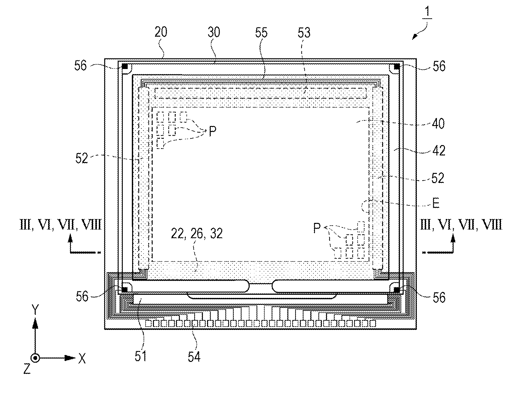
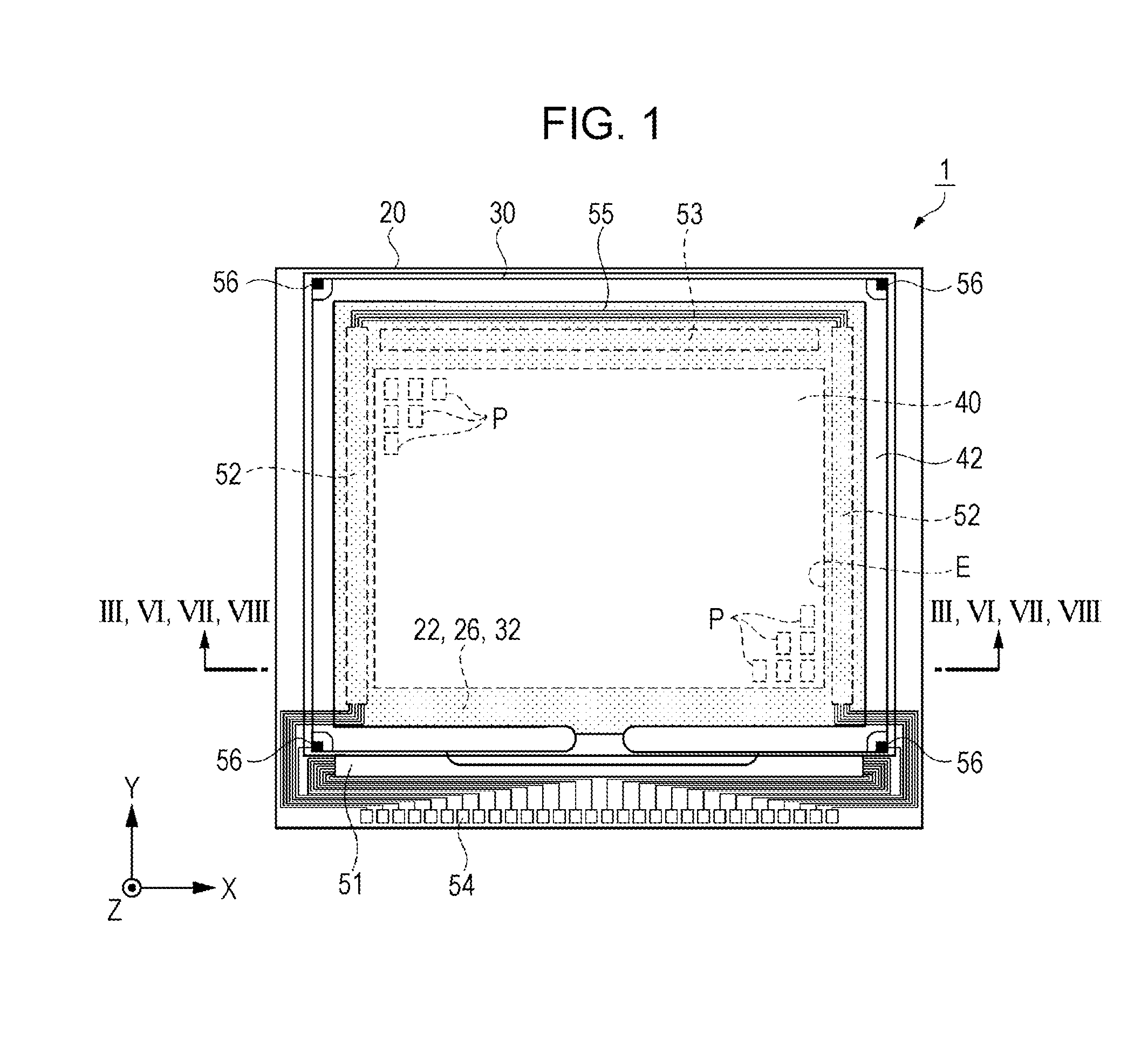
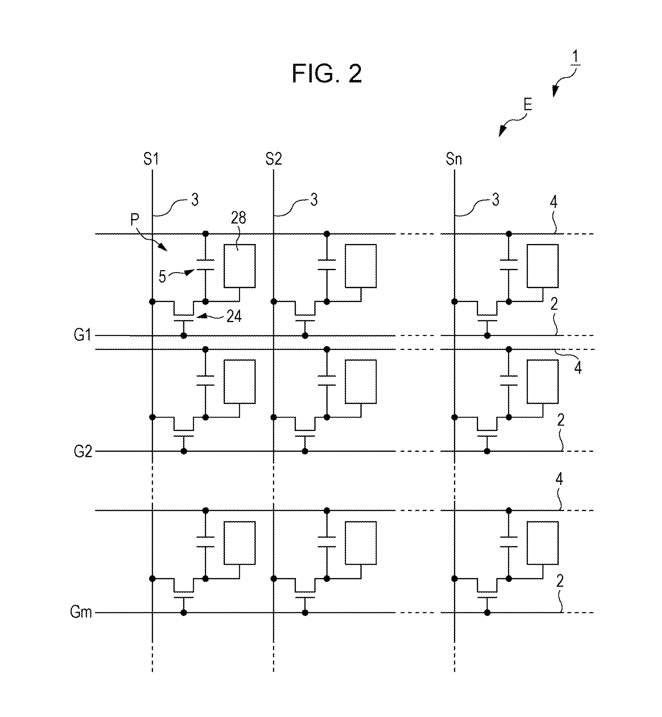
[0051]First, the liquid crystal device as the electro-optical apparatus according to the first embodiment will be described with reference to FIG. 1 to FIG. 3. FIG. 1 is a schematic plan view illustrating a configuration of a liquid crystal device according to a first embodiment. FIG. 2 is an equivalent circuit diagram illustrating an electrical configuration of the liquid crystal device according to the first embodiment. FIG. 3 is a schematic cross-sectional view illustrating a configuration of the liquid crystal device according to the first embodiment. For details, FIG. 3 is a schematic cross...

second embodiment

[0135]The liquid crystal device according to the second embodiment is almost the same configuration as that of the first embodiment except that the micro lens ML1 and the micro lens ML2 in the element substrate are configured in a different way from each other. Here, the difference with respect to the first embodiment will be described. FIG. 9 is a schematic cross-sectional view illustrating the configuration of liquid crystal device according to the second embodiment. The same constituent elements as in the first embodiment are given the same reference numerals, and repeated description will be omitted.

Substrate for Electro-Optical Apparatus

[0136]As shown in FIG. 9, a liquid crystal device 1A according to the second embodiment is provided with an element substrate 20A as the substrate for electro-optical apparatus. The element substrate 20A according to the second embodiment is provided with a micro lens ML1A as the first micro lens and a micro lens ML2A as the second micro lens on...

third embodiment

[0143]The liquid crystal device according to the third embodiment is provided with a first substrate having the micro lens ML1, and a second substrate having the micro lens ML2 on the element substrate, and is almost the same configuration as that of the first embodiment except that the first substrate and the second substrate are joined to each other via the adhesive layer. Here, the difference with respect to the first embodiment will be described. FIG. 10 is a schematic cross-sectional view illustrating the configuration of liquid crystal device according to the third embodiment. The same constituent elements as in the first embodiment are given the same reference numerals, and repeated description will be omitted.

Substrate for Electro-Optical Apparatus

[0144]As shown in FIG. 10, a liquid crystal device 1B according to the third embodiment is provided with an element substrate 20B as the substrate for electro-optical apparatus. The element substrate 20B according to the third embo...


PUM

PropertyMeasurementUnit
areaaaaaaaaaaa
refractive poweraaaaaaaaaa
electricallyaaaaaaaaaa

Abstract

An element substrate is provided with a substrate; a pixel electrode; a light shielding layer which is disposed between the substrate and the pixel electrode and has an opening in an area overlapping with the pixel electrode; a TFT that is disposed between the light shielding layer and the pixel electrode has a channel area which is disposed in an area overlapping with the light shielding layer; a light shielding layer that is disposed between the TFT and the pixel electrode and has an opening in an area overlapping with the pixel electrode; a micro lens that is disposed between the substrate and the light shielding layer and disposed in an area overlapping with the pixel electrode; and a micro lens that is disposed between the light shielding layer and the pixel electrode and disposed in an area overlapping with the pixel electrode.

Description

BACKGROUND[0001]1. Technical Field[0002]The present invention is related to a substrate for electro-optical apparatus, an electro-optical apparatus, and electronic equipment.[0003]2. Related Art[0004]An electro-optical apparatus is well known that an electro optical substance such as a liquid crystal is provided between an element substrate and a counter substrate. As the electro-optical apparatus, a liquid crystal device, which is used as a liquid crystal light valve of a projector, can be exemplified. In the liquid crystal device, a light shielding layer is provided in an area in which a switching element, a wiring, or the like is disposed, and a part of the light to be incident is shielded in the light shielding layer not to be used. Thus, a configuration is well known that a micro lens is provided on one substrate so as to use the light being shielded in the light shielding layer by condensing the light incident on the liquid crystal device.[0005]However, when refractive power o...

Claims


Application Information

Patent Timeline
Patent Type & Authority Applications(United States)
IPC IPC(8): H01L33/58H01L27/12
CPCH01L27/1214H01L33/58H01L29/78633H01L27/1218H01L27/124G02F1/133526G02F1/136209G02F1/136227
Inventor NIMURA, TORU
Owner SEIKO EPSON CORP
Why Eureka
Try Eureka