
Compensation accuracy

a technology of compensation accuracy and luminance, applied in the field of display technology, can solve the problems of affecting the quality of output in an oled based pixel, and the inability to achieve the desired higher luminance level for more effective compensation while within the parameters of image data

Active Publication Date: 2015-02-12
IGNIS INNOVATION
View PDF32 Cites 23 Cited by
  • Summary
  • Abstract
  • Description
  • Claims
  • Application Information

AI Technical Summary

Benefits of technology

The patent describes a system that divides compensation data among multiple frames and uses it to compensate image data in each frame. This helps to reduce the value needed for calibration by using the values from all the frames. The result is improved image quality and reduced calibration requirements.

Problems solved by technology

However, the quality of output in an OLED based pixel is affected by the properties of a drive transistor that is typically fabricated from amorphous or poly silicon as well as the OLED itself.
However, luminance levels are largely dictated by the level of brightness for the image data to a pixel, and the desired higher levels of luminance for more effective compensation may not be achievable while within the parameters of the image data.

Method used


Image

  • Compensation accuracy
  • Compensation accuracy
  • Compensation accuracy

Examples


first embodiment

[0088]FIG. 19 illustrates a first embodiment, in which:[0089]1) The frame is divided into two or more sub-frames 191 and 192 (or two or more consecutive frames are used as one set of sub-frames).[0090]2) The compensation data is applied to at least one of the sub-frames.[0091]3) The video sub-frames and compensation sub-frames are different.[0092]4) Thus, both video and compensation data can be as large as data resolution of the driver.[0093]5) The sub-frames can have different size. For example, the video sub-frame can be longer than the compensation sub-frame. This results in less brightness reduction because of using part of the frame for compensation. It also results in smaller steps for compensation due to the smaller sub-frame, which can improve the external compensation accuracy.

second embodiment

[0094]FIG. 20 illustrates a second embodiment, in which:[0095]1) The frame is divided into two or more sub frames 201 and 202.[0096]2) The compensation data is applied to at least one of the sub-frames 201.[0097]3) If the video calibrated data is larger than the data resolution of the driver, the extra data can be transferred to the other sub-frame 202 (left-over sub-frame).[0098]4) There can be multiple left-over sub-frames.[0099]5) The sub-frames can have different sizes.

third embodiment

[0100]FIG. 21 illustrates a third embodiment, in which:[0101]1) The frame is divided into two or more sub-frames 211 and 212.[0102]2) The compensation data is divided between sub-frames (this division can be with different weights, but the best visual effect is achieved when the video is divided by sub-frames equally and the residue value is applied to one or more than one sub-frame).[0103]3) The sub-frames can have different sizes.

[0104]Time Division Compensation

[0105]FIG. 22 illustrates a first embodiment, in which the calibrated video data 221, which is the video data manipulated with the compensation data, is in two or more frames. For example, if two frames are used for this purpose, the calibrated data is divided by two and each frame contains half of the calibrated data. The residue of the division can be shown in either of the frames. For example, if the calibrated data is 311, one frame contains 155 and the other frame contains 156.

[0106]Step 222 determines whether there is...


PUM


Abstract

A system uses image data, representing images to be displayed in successive frames, to drive a display having pixels that include a drive transistor and an organic light emitting device by dividing each frame into at least first and second sub-frames, supplying the image data during one of the sub-frames, supplying compensation data during the other of the sub-frames, compensating image data based on the compensation data, and supplying each pixel with a drive current that is based on the compensated image data during each frame. The compensated image data may be supplied from a driver having a preselected data resolution, and the system determines whether the compensated image data is greater than the data resolution of the driver, and if the compensated image data is greater than the data resolution of the driver, transfers the excess compensated image data to a different sub-frame.

Description

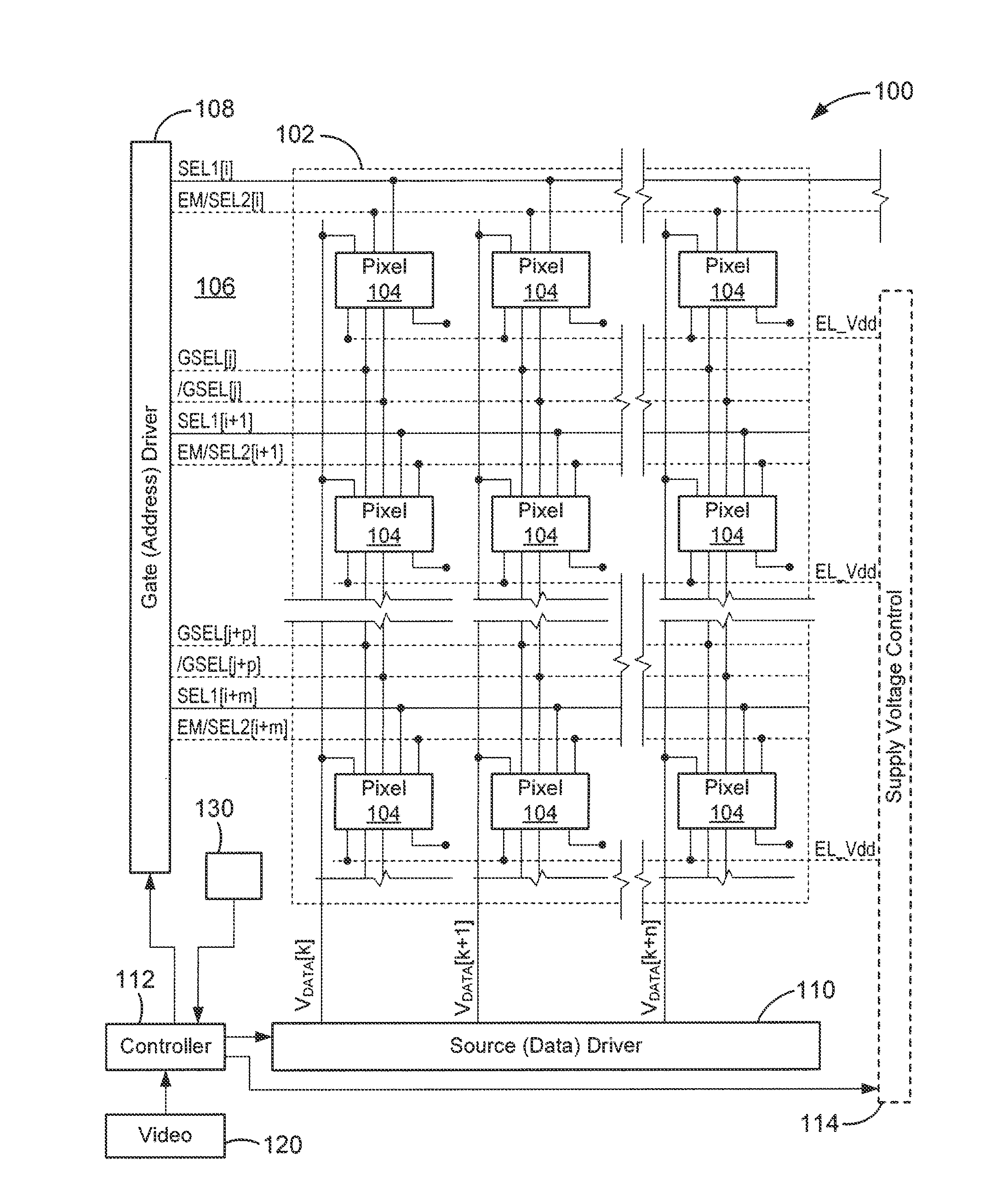
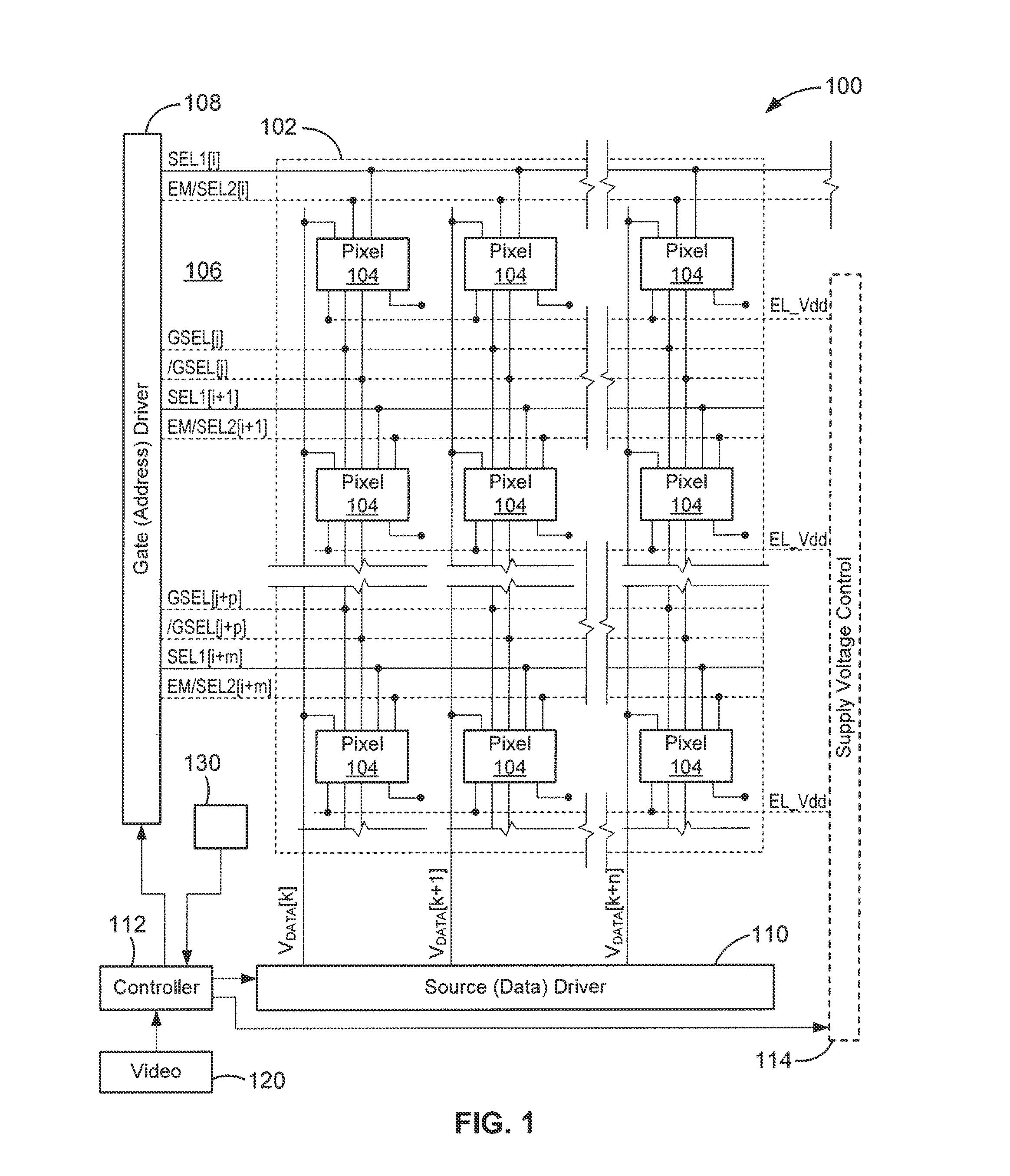
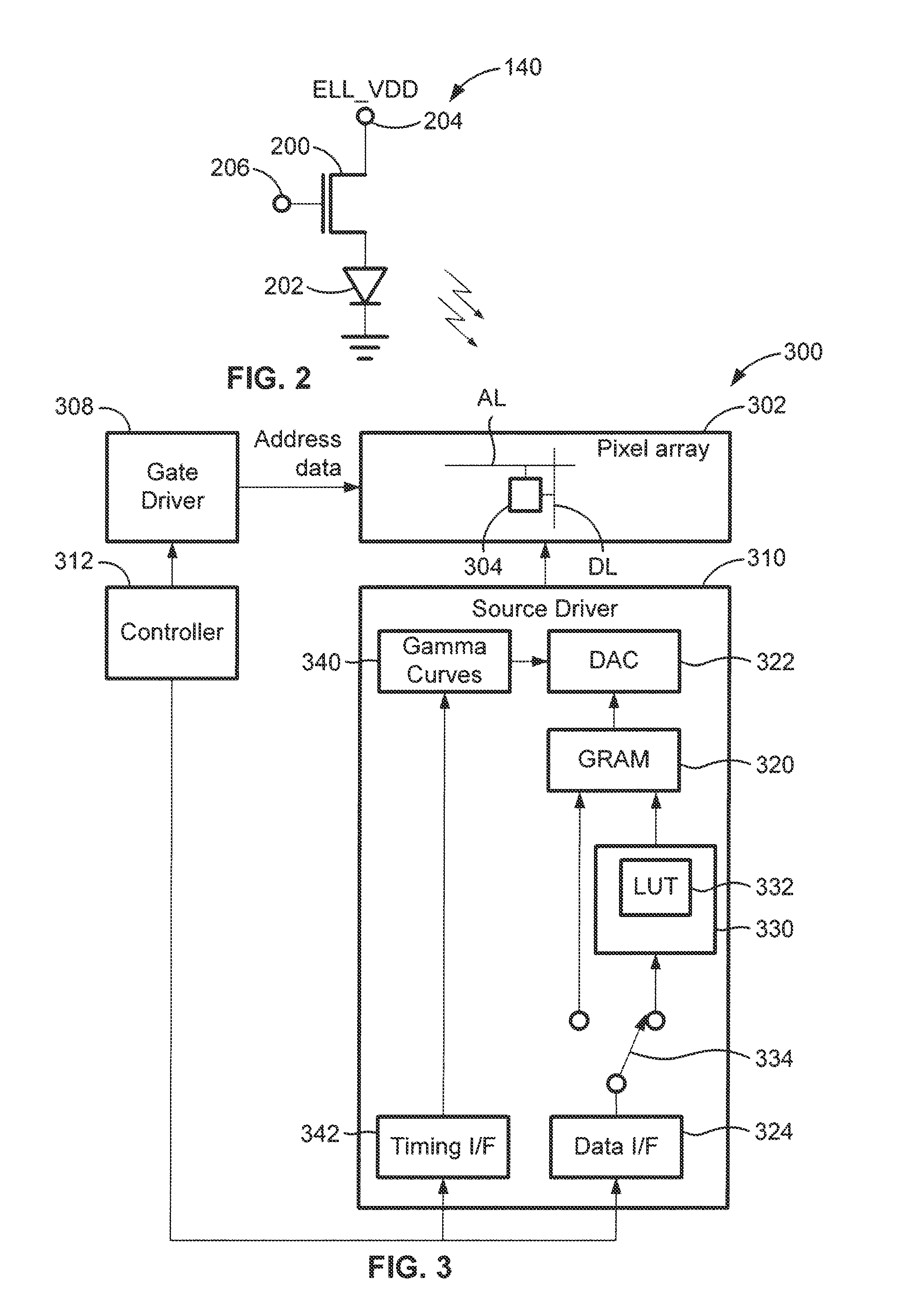
CROSS REFERENCE TO RELATED APPLICATION[0001]This application claims the benefit of U.S. Provisional Patent Application No. 61 / 864,972, filed Aug. 12, 2013, which is hereby incorporated by reference in its entirety.FIELD OF INVENTION[0002]The present invention relates to display technology, and particularly to driving systems for active-matrix displays such as AMOLED displays.BACKGROUND OF THE INVENTION[0003]A display device having a plurality of pixels (or sub-pixels) arranged in a matrix has been widely used in various applications. Such a display device includes a panel having the pixels and peripheral circuits for controlling the panels. Typically, the pixels are defined by the intersections of scan lines and data lines, and the peripheral circuits include a gate driver for scanning the scan lines and a source driver for supplying image data to the data lines. The source driver may include a gamma correction circuit for controlling the gray scale of each pixel. In order to displa...

Claims


Application Information

Patent Timeline
Patent Type & Authority Applications(United States)
IPC IPC(8): G09G3/32G09G3/20
CPCG09G3/3233G09G3/2022G09G2300/0819G09G2320/043G09G2320/0626G09G2320/045H10K59/123G09G3/3266G09G3/3291G09G2300/0809G09G2320/0646
Inventor CHAJI, GHOLAMREZAZAHIROVIC, NINO
Owner IGNIS INNOVATION
Learn More