Chip package and method for fabricating the same

a technology of chip and packaging, applied in the field of semiconductor devices, can solve the problems of large chip warpage, solder ball on the chip not being able to bond to the packaging substrate, and the form of chip packages with more functions and smaller sizes has become an important issue, so as to reduce the possibility of image distortion

Inactive Publication Date: 2015-04-09
XINTEC INC
View PDF16 Cites 13 Cited by
  • Summary
  • Abstract
  • Description
  • Claims
  • Application Information

AI Technical Summary

Benefits of technology

[0025]In the aforementioned embodiments of the present invention, since the conductive structures have different heights and the heights of the conductive structures are gradually increased from the central region of the semiconductor chip to the edge region of the semiconductor chip, the distance between the edge region of the semiconductor chip and the packaging structure is greater than the di

Problems solved by technology

Due to reductions in the size of electronic products, forming chip packages with more functions and smaller sizes has become an important issue.
However, chip packages with more functions and smaller sizes have high-density circuits, which results in a large chip warpage and can lead to some of the solder balls

Method used


Image

  • Chip package and method for fabricating the same
  • Chip package and method for fabricating the same
  • Chip package and method for fabricating the same

Examples


Embodiment Construction

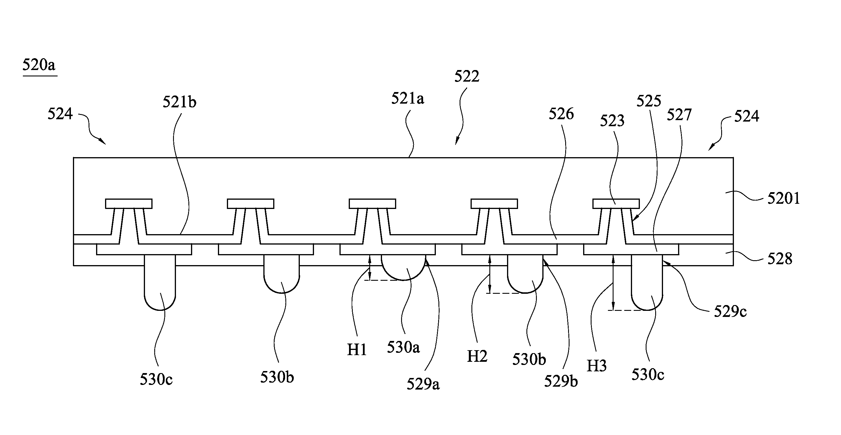
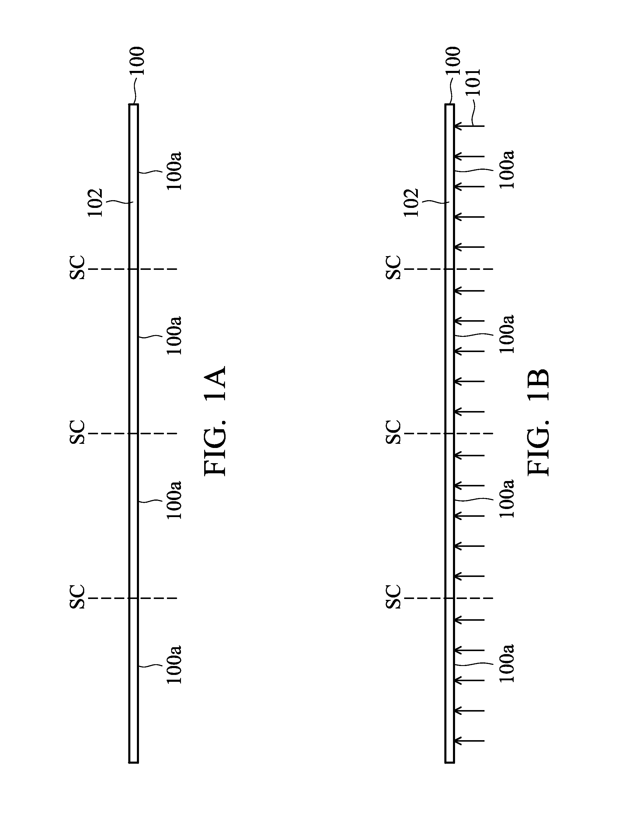
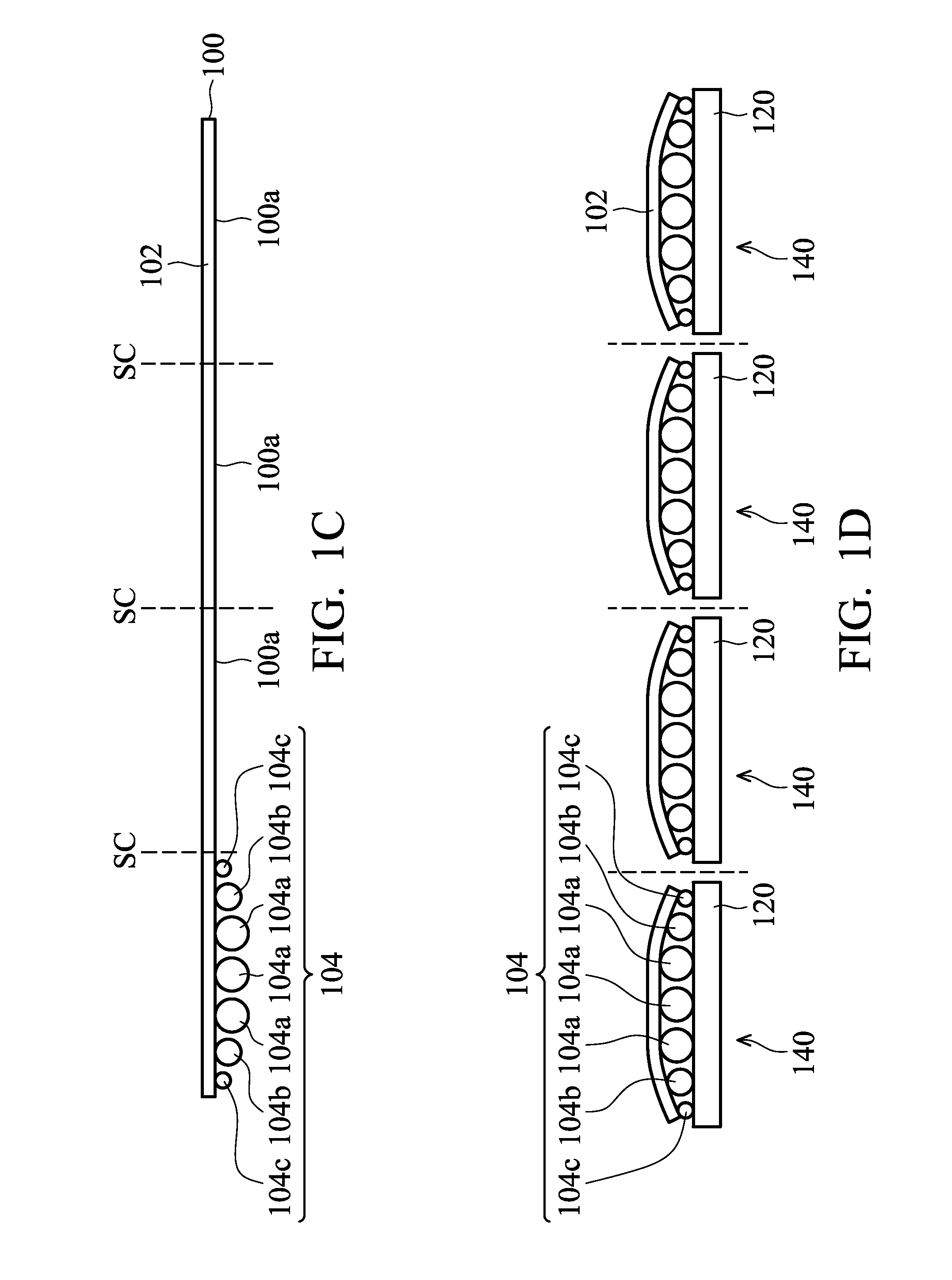
[0044]Reference will now be made in detail to the present embodiments of the invention, examples of which are illustrated in the accompanying drawings. Wherever possible, the same reference numbers are used in the drawings and the description to refer to the same or like parts.

[0045]It should be understood that the following disclosure provides many different embodiments, or examples, for implementing different features of the invention. Specific examples of components and arrangements are described below to simplify the present disclosure. These are, of course, merely examples and are not intended to be limiting. In addition, the present disclosure may repeat reference numbers and / or letters in the various examples. This repetition is for the purpose of simplicity and clarity and does not in itself dictate a relationship between the various embodiments and / or configurations discussed. Furthermore, descriptions of a first layer “on,”“overlying,” (and like descriptions) a second laye...


PUM


Abstract

A chip package includes a packaging substrate, a semiconductor chip, and a plurality of conductive structures. The semiconductor chip has a central region and an edge region that surrounds the central region. The conductive structures are between the packaging substrate and the semiconductor chip. The conductive structures have different heights, and the heights of the conductive structures are gradually increased from the central region of the semiconductor chip to the edge region of the semiconductor chip, such that a distance between the edge region of the semiconductor chip and the packaging substrate is greater than a distance between the central region of the semiconductor chip and the packaging substrate.

Description

RELATED APPLICATIONS[0001]This application is a Continuation-in-part of U.S. application Ser. No. 14 / 251,470, filed on Apr. 11, 2014, which claims priority of U.S. provisional Application Ser. No. 61 / 811,487, filed on Apr. 12, 2013, the entirety of which is incorporated by reference herein.BACKGROUND[0002]1. Field of Invention[0003]The invention relates to a semiconductor device, and in particular relates to a chip package and fabrication method thereof.[0004]2. Description of Related Art[0005]The chip packaging process is an important process when fabricating an electronic product. Chip packages not only provide chips with protection from environmental contaminants, but also provide an interface for connection between electronic elements in the chips and electronic elements outside of the chip package.[0006]Due to reductions in the size of electronic products, forming chip packages with more functions and smaller sizes has become an important issue. However, chip packages with more...

Claims


Application Information

Patent Timeline
IPC IPC(8): H01L23/00
CPCH01L24/17H01L24/81H01L24/11H01L2224/1703H01L2224/11312H01L2224/16055H01L2224/16052H01L2224/13024H01L2224/16227H01L21/6835H01L21/6836H01L22/12H01L22/20H01L24/02H01L24/13H01L24/14H01L24/16H01L24/92H01L24/94H01L24/97H01L27/14618H01L27/14636H01L2221/68327H01L2221/68386H01L2224/0231H01L2224/0235H01L2224/02377H01L2224/11002H01L2224/11334H01L2224/13012H01L2224/13014H01L2224/13022H01L2224/131H01L2224/1403H01L2224/14051H01L2224/14131H01L2224/14136H01L2224/14145H01L2224/14177H01L2224/14179H01L2224/16058H01L2224/17051H01L2224/17517H01L2224/17519H01L2224/81191H01L2224/81815H01L2224/81986H01L2224/92H01L2224/94H01L2224/97H01L2924/01322H01L2924/12042H01L2924/13091H01L2924/1461H01L2924/3511H01L2924/00H01L2924/014H01L2224/14146H01L2224/81H01L2224/81907H01L21/78H01L2924/00012H01L2224/11H01L2924/00014
Inventor SUEN, WEI-LUENLIN, CHIA-SHENGHO, YEN-SHIHLIU, TSANG-YU
Owner XINTEC INC
Why Eureka
Try Eureka