Mask for depositing thin film, method of manufacturing organic light emitting diode display using the same, and organic light emitting diode display using the same

a technology of light-emitting diodes and masks, which is applied in the field of masks for depositing thin films, can solve problems such as limitation in accuracy, and achieve the effects of reducing shadows, reducing deformation of opening patterns, and improving resolution

Inactive Publication Date: 2015-04-16
SAMSUNG DISPLAY CO LTD
View PDF3 Cites 14 Cited by
  • Summary
  • Abstract
  • Description
  • Claims
  • Application Information

AI Technical Summary

Benefits of technology

[0030]When the aforementioned mask for the depositing the thin film is used, shadow is reduced so that it is possible to decr

Problems solved by technology

However, in a case where the organic light emitting diode display is manufactured by using the aforementioned mask, the organic light emitting diode display with high resolution uses a ma

Method used


Image

  • Mask for depositing thin film, method of manufacturing organic light emitting diode display using the same, and organic light emitting diode display using the same
  • Mask for depositing thin film, method of manufacturing organic light emitting diode display using the same, and organic light emitting diode display using the same
  • Mask for depositing thin film, method of manufacturing organic light emitting diode display using the same, and organic light emitting diode display using the same

Examples


Embodiment Construction

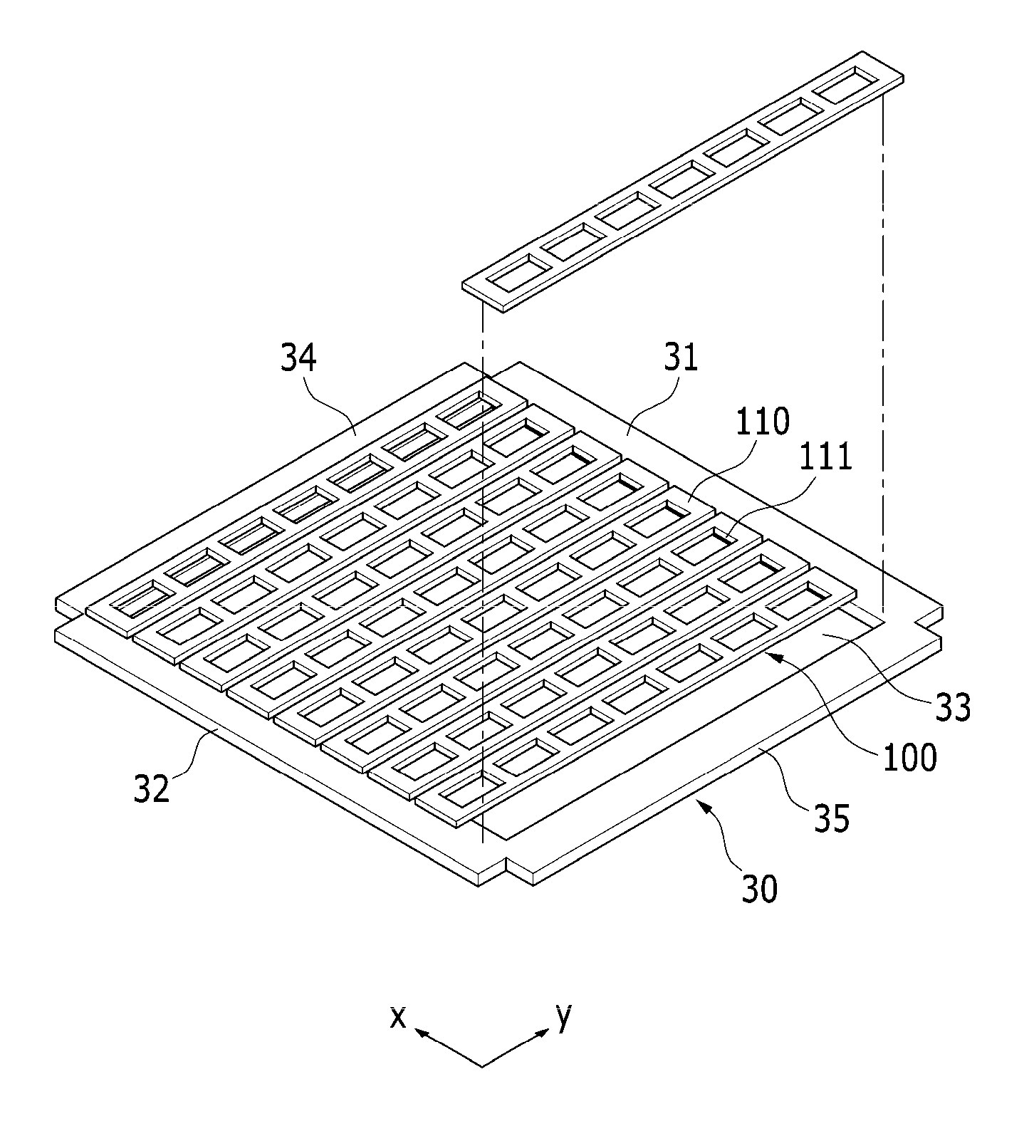
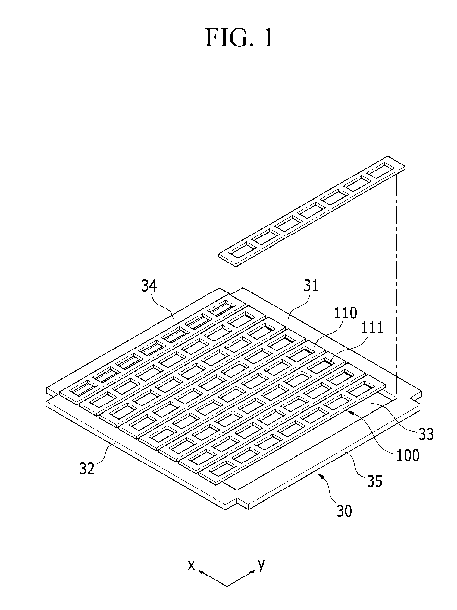
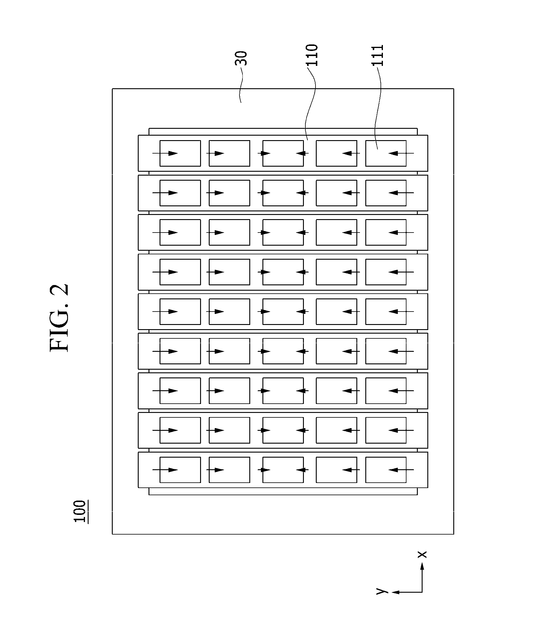
[0038]In the following detailed description, only certain exemplary embodiments of the present invention have been shown and described, simply by way of illustration. As those skilled in the art would realize, the described embodiments may be modified in various different ways, all without departing from the spirit or scope of the present invention. The drawings and description are to be regarded as illustrative in nature and not restrictive. Like reference numerals designate like elements throughout the specification.

[0039]In describing each drawing, similar reference numerals are used for similar constituent elements. In the accompanying drawings, sizes of structures are enlarged compared to actual sizes for illustration for accuracy of the present invention. Accordingly, the drawings are not necessarily to scale. Although the terms first, second, third, etc. may be used herein to describe various constituent elements, they are not limited thereto. The terms are used only for the ...


PUM


Abstract

A mask for depositing a thin film according to an exemplary embodiment of the present invention includes: mask strips each including a plurality of pattern portions disposed end to end along one direction; and a frame on which the mask strips are positioned. Intervals between adjacent ends of adjacent pattern portions differ from each other according to distance from a predetermined location, thereby providing an organic light emitting diode display having a more uniform quality.

Description

CROSS-REFERENCE TO RELATED APPLICATION[0001]This application claims priority to, and the benefit of, Korean Patent Application No. 10-2013-0121463 filed in the Korean Intellectual Property Office on Oct. 11, 2013, the entire contents of which are incorporated herein by reference.BACKGROUND[0002](a) Field[0003]Embodiments of the present invention relate generally to organic light emitting diode displays. More specifically, embodiments of the present invention relate to a mask for depositing a thin film, a method of manufacturing an organic light emitting diode display using the same, and an organic light emitting diode display using the same.[0004](b) Description of the Related Art[0005]A display device is a device displaying an image, one display utilizing such a device being an organic light emitting diode display.[0006]The organic light emitting diode display has a self light emitting characteristic, and does not require a separate light source, unlike a liquid crystal display. Ac...

Claims


Application Information

Patent Timeline
IPC IPC(8): H01L51/00B05C21/00H01L51/52H01L51/56H01L27/32
CPCH01L51/0012H01L51/56H01L27/32H01L51/5203B05C21/005H10K59/35H10K71/166H10K71/00H05B33/10
Inventor LEE, CHOONG HO
Owner SAMSUNG DISPLAY CO LTD
Why Eureka
Try Eureka