Display device

a display device and display technology, applied in the field of display devices, can solve the problems of display defects, difficult to set a common voltage, and increase the asymmetry between positive polarity and negative polarity, and achieve the effect of reducing the luminance difference between the edge portion and the center portion of the pixel region of the display devi

Inactive Publication Date: 2015-06-04
SAMSUNG DISPLAY CO LTD
View PDF1 Cites 6 Cited by
  • Summary
  • Abstract
  • Description
  • Claims
  • Application Information

AI Technical Summary

Benefits of technology

[0030]According to exemplary embodiments of the present invention, the difference in luminance between the edge portion and the center portion of the pixel region of the display device may be reduced.

Problems solved by technology

However, when using this method, it may be difficult to set a common voltage.
In this case, if the common voltage is set based on the case in which a low-gradation image is displayed, asymmetry between positive polarity and negative polarity may be increased when the high-gradation image is displayed, and display defects such as, for example, ghosting and crosstalk may occur.
However, if the common voltage is set to a low value, luminance of a center portion of a pixel region of the display device may become heightened due to delay phenomenon of a gate signal.

Method used


Image

  • Display device
  • Display device
  • Display device

Examples


Embodiment Construction

[0045]Exemplary embodiments of the present invention will be described more fully hereinafter with reference to the accompanying drawings. Like reference numerals may refer to like elements throughout the accompanying drawings.

[0046]It will be understood that when an element or layer is referred to as being “on,” or “connected to” another element or layer, it can be directly on or connected to the other element or layer, or intervening elements or layers may be present.

[0047]Spatially relative terms, such as “below,”“beneath,”“lower,”“above,”“upper,” etc., may be used herein for ease of description to describe one element or feature's relationship to another element(s) or feature(s) as illustrated in the figures. It will be understood that the spatially relative terms are intended to encompass different orientations of the device in use or operation in addition to the orientation depicted in the figures.

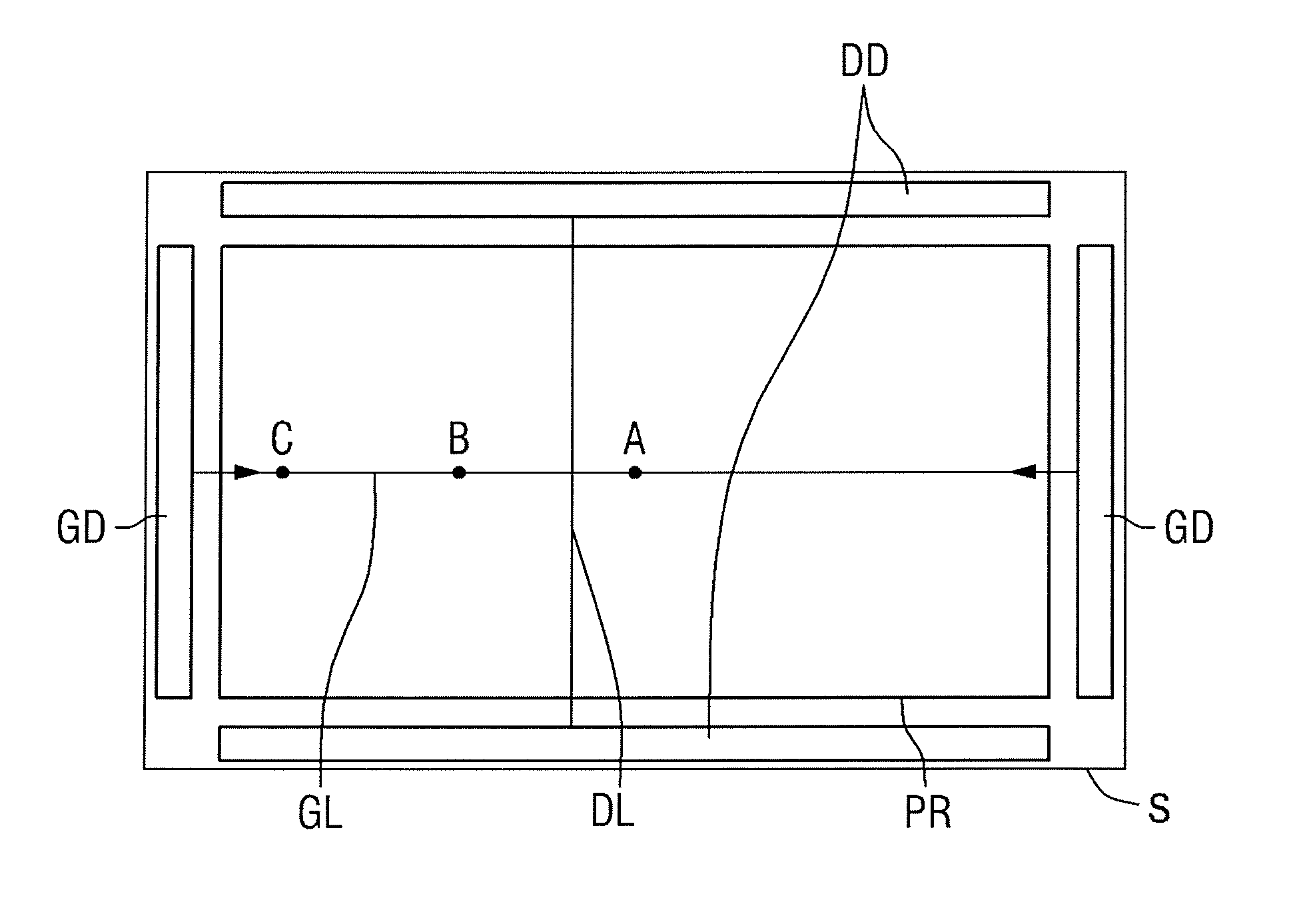
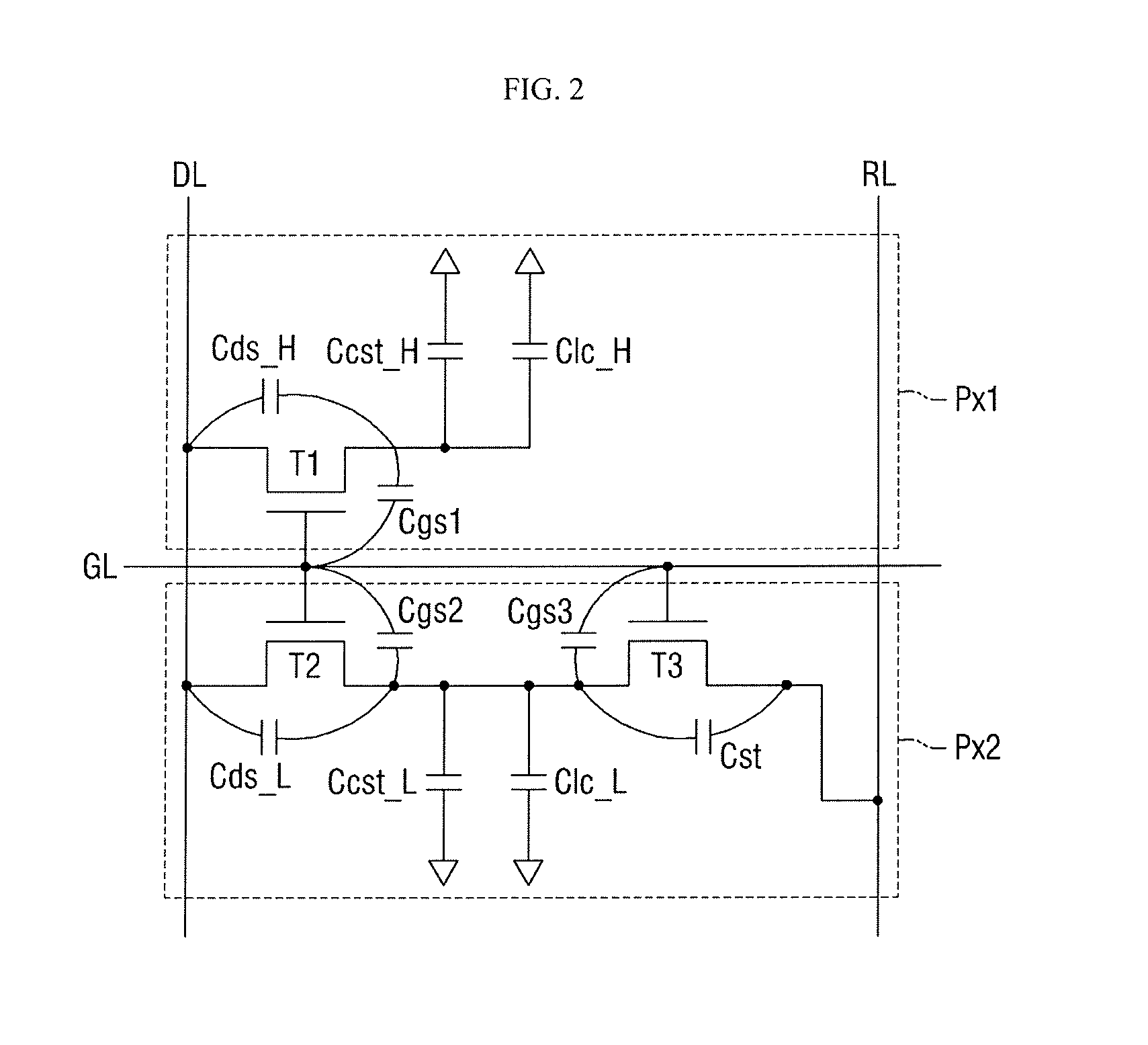
[0048]A display device is a device that displays an image. A display device may ...


PUM


Abstract

A display device includes a substrate, a gate line connected to a gate driver, a reference voltage line, a data line crossing the gate line and the reference voltage line, a first thin film transistor including a first drain electrode and connected to the gate line and the data line, a second thin film transistor including a second drain electrode, a third thin film transistor connected to the gate line, the reference voltage line, and the second thin film transistor, and a pixel electrode including a first sub-pixel electrode connected to the first thin film transistor and a second sub-pixel electrode connected to the second thin film transistor. The first drain electrode overlaps the reference voltage line, and an area of a region in which the first drain electrode and the reference voltage line overlap each other increases in a direction toward the gate driver.

Description

CROSS-REFERENCE TO RELATED APPLICATIONS[0001]This application claims priority under 35 U.S.C. §119 to Korean Patent Application No. 10-2013-0150010 filed on Dec. 4, 2013, the disclosure of which is incorporated by reference herein in its entirety.TECHNICAL FIELD[0002]The present invention relates to a display device.DISCUSSION OF THE RELATED ART[0003]A display device is a device that visually displays data. The display device may be, for example, a liquid crystal display, an electrophoretic display, an organic light emitting display, an inorganic EL (electro luminescent) display, a field emission display, a surface-conduction electron-emitter display, a plasma display, or a cathode ray display.[0004]A liquid crystal display includes two display substrates on which electric field generating electrodes, such as a pixel electrode and a common electrode, are formed, and a liquid crystal layer disposed between the electric field generating electrodes. An electric field is generated by ap...

Claims


Application Information

Patent Timeline
Patent Type & Authority Applications(United States)
IPC IPC(8): G09G5/00
CPCG09G2300/0426G09G5/00G02F1/13306G02F1/136213G02F1/136286G02F1/1368G09G3/3614G09G3/3655G09G2300/043G09G2300/0823G02F1/1343G09F9/30G02F1/13624G02F1/136245
Inventor LEE, SEUNG KYUSOHN, WOO SUNGCHO, YONG TAE
Owner SAMSUNG DISPLAY CO LTD
Why Eureka
Try Eureka