Coating a substrate web by atomic layer deposition

a technology of atomic layer deposition and substrate, which is applied in the direction of chemical vapor deposition coating, coating, metal material coating process, etc., can solve the problem of 1% non-uniformity over the substrate wafer

Inactive Publication Date: 2015-06-18
PICOSUN OY
View PDF2 Cites 245 Cited by
  • Summary
  • Abstract
  • Description
  • Claims
  • Application Information

AI Technical Summary

Benefits of technology

[0013]inputting the substrate web from an excess pressure volume into the reaction space

Problems solved by technology

For example, in an experiment aluminum oxide has been grown by thermal ALD from trimethylaluminum (CH3)3Al, als

Method used


Image

  • Coating a substrate web by atomic layer deposition
  • Coating a substrate web by atomic layer deposition
  • Coating a substrate web by atomic layer deposition

Examples


Embodiment Construction

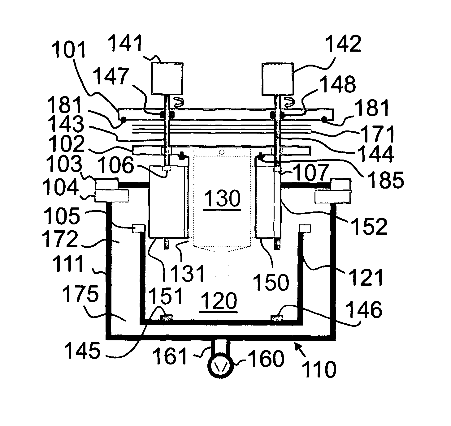
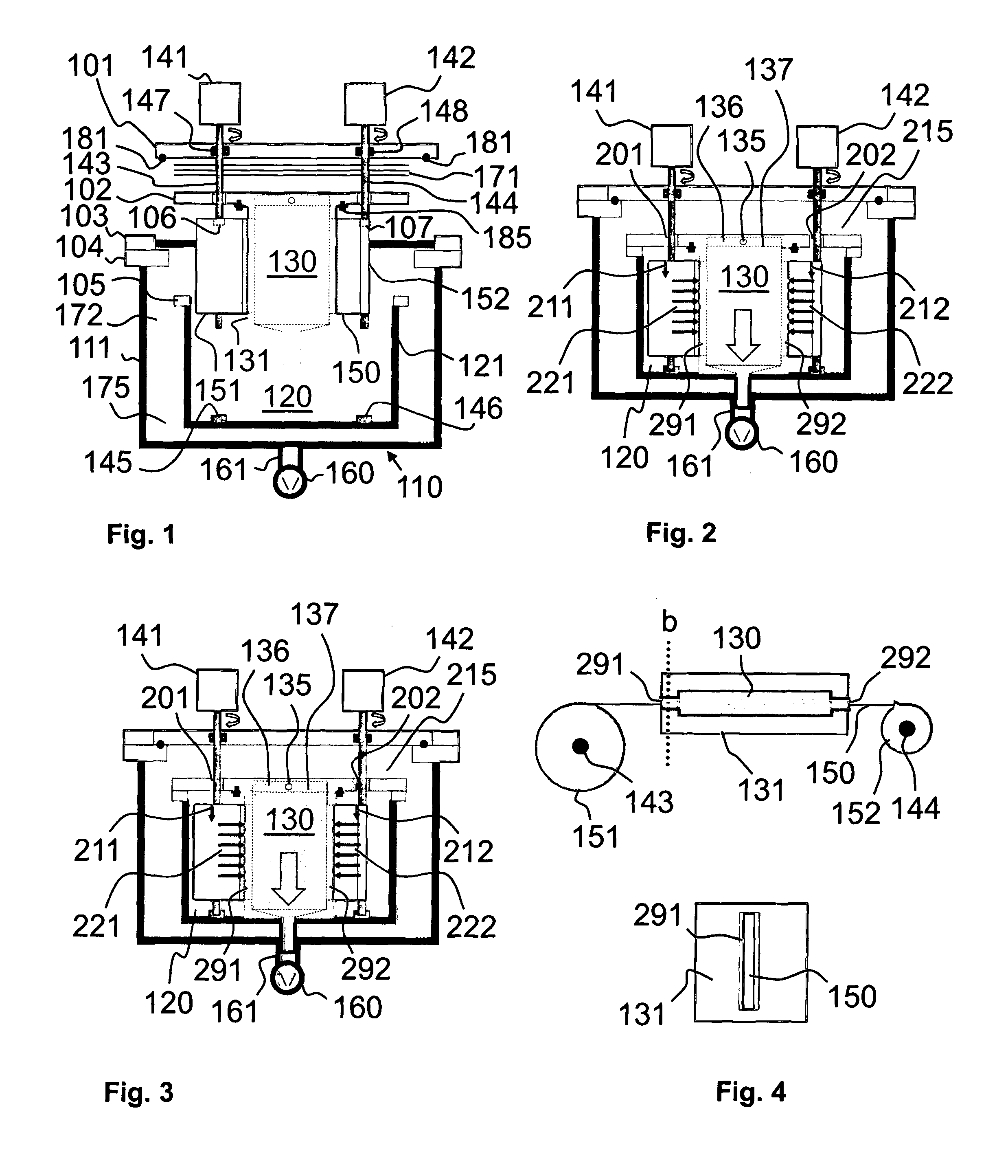
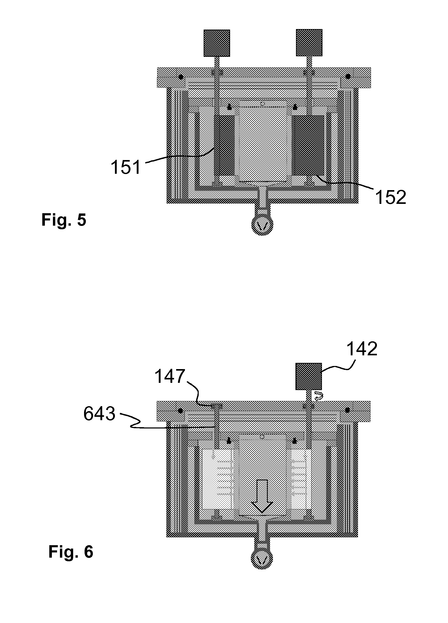
[0096]In the following description, Atomic Layer Deposition (ALD) technology is used as an example. The basics of an ALD growth mechanism are known to a skilled person. As mentioned in the introductory portion of this patent application, ALD is a special chemical deposition method based on the sequential introduction of at least two reactive precursor species to at least one substrate. The substrate, or the moving substrate web in this case, is located within a reaction space. The reaction space is typically heated. The basic growth mechanism of ALD relies on the bond strength differences between chemical adsorption (chemisorption) and physical adsorption (physisorption). ALD utilizes chemisorption and eliminates physisorption during the deposition process. During chemisorption a strong chemical bond is formed between atom(s) of a solid phase surface and a molecule that is arriving from the gas phase. Bonding by physisorption is much weaker because only van der Waals forces are invo...


PUM

PropertyMeasurementUnit
Thicknessaaaaaaaaaa
Pressureaaaaaaaaaa
Flow rateaaaaaaaaaa

Abstract

The present invention relates to a method of driving a substrate web (950) into a reaction space of an atomic layer deposition (ALD) reactor and apparatuses therefore. The invention includes driving a substrate web into a reaction space (930) of an atomic layer deposition reactor, and exposing the reaction space to precursor pulses to deposit material on said substrate web by sequential self-saturating surface reactions. One effect of the invention is a simpler structure compared to earlier spatial roll-to-roll ALD reactors. Another effect is that the thickness of deposited material is directly determined by the speed of the web.

Description

FIELD OF THE INVENTION[0001]The present invention generally relates to deposition reactors. More particularly, the invention relates to atomic layer deposition reactors in which material is deposited on surfaces by sequential self-saturating surface reactions.BACKGROUND OF THE INVENTION[0002]Atomic Layer Epitaxy (ALE) method was invented by Dr. Tuomo Suntola in the early 1970's. Another generic name for the method is Atomic Layer Deposition (ALD) and it is nowadays used instead of ALE. ALD is a special chemical deposition method based on the sequential introduction of at least two reactive precursor species to at least one substrate.[0003]Thin films grown by ALD are dense, pinhole free and have uniform thickness. For example, in an experiment aluminum oxide has been grown by thermal ALD from trimethylaluminum (CH3)3Al, also referred to as TMA, and water at 250-300° C. resulting in only about 1% non-uniformity over a substrate wafer.[0004]Until now the ALD industry has mainly concent...

Claims


Application Information

Patent Timeline
IPC IPC(8): C23C16/455C23C16/54
CPCC23C16/54C23C16/45544C23C16/45525C23C16/545C23C16/403
Inventor LINDFORS, SVEN
Owner PICOSUN OY
Why Eureka
Try Eureka